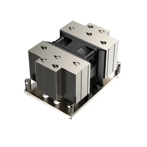
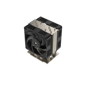
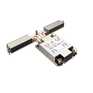
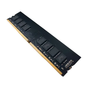
Engineered for high power density applications, ensuring peak operational performance under demanding thermal constraints.
Tokyo serves as a global epicentre for high-tech manufacturing, advanced robotics, autonomous vehicle systems, and high-frequency communication infrastructures. The metropolitan area, including Ota City's precision manufacturing clusters and the technology design hubs of Kanagawa and Saitama, generates significant demand for robust electronic systems. At the core of these systems lies the printed circuit board (PCB), which must survive increasingly hostile operational environments.
Standard FR-4 PCBs have a glass transition temperature (Tg) of 130°C to 140°C. In high-performance, high-power environments typical of modern industrial controls, Tokyo’s smart city grids, and server clusters, these standard boards risk thermal delamination, pad lifting, and excessive Z-axis expansion. High-TG PCBs (Tg ≥ 170°C) offer the thermal stability and mechanical integrity required to withstand lead-free reflow profile requirements and constant high-temperature operations.
The Glass Transition Temperature represents the point at which a polymer matrix shifts from a hard, rigid state to a rubbery, compliant state. For electronics operating continuously, reaching this temperature ruins structural support, resulting in micro-cracks along through-hole vias, copper trace fatigue, and component failures. High-TG materials ensure the board retains its mechanical rigidity, low dielectric loss, and high insulation resistance during thermal cycles.
High-TG substrates feature lower Coefficient of Thermal Expansion (CTE) along the Z-axis, protecting multi-layer vias from stress fractures caused by high operating temperatures.
RoHS standards demand lead-free reflow temperatures (exceeding 255°C). High-TG laminates are designed to survive these profiles without physical degradation.
Exhibiting high resistance to Conductive Anodic Filament (CAF) growth, our boards prevent tracking shorts in humid conditions typical of Japanese summers.
Thermal mitigation platforms designed to interface directly with High-TG PCBs for enterprise deployment.
Choosing the correct PCB grade is necessary to avoid physical failures and signal attenuation. When serving the Tokyo market, our products comply with JIS and international standards. The table below details the performance differences across classes:
| Property | Standard FR-4 | Medium-TG FR-4 | High-TG FR-4 (Target Standard) |
|---|---|---|---|
| Glass Transition Temp (Tg) | 130°C - 140°C | 150°C - 160°C | 170°C - 180°C+ |
| Decomposition Temp (Td) | ≤ 310°C | ≤ 325°C | ≥ 340°C (High thermal safety) |
| Z-Axis CTE (Before Tg) | 55 - 60 ppm/°C | 50 - 55 ppm/°C | 40 - 45 ppm/°C (Lower thermal stress) |
| Z-Axis CTE (After Tg) | 270 - 300 ppm/°C | 250 - 270 ppm/°C | 220 - 240 ppm/°C |
| T260 / T288 Delamination Time | < 30 mins / < 5 mins | > 45 mins / > 10 mins | > 60 mins / > 15 mins (Highly reliable) |
| Flammability Rating | UL 94 V-0 | UL 94 V-0 | UL 94 V-0 |
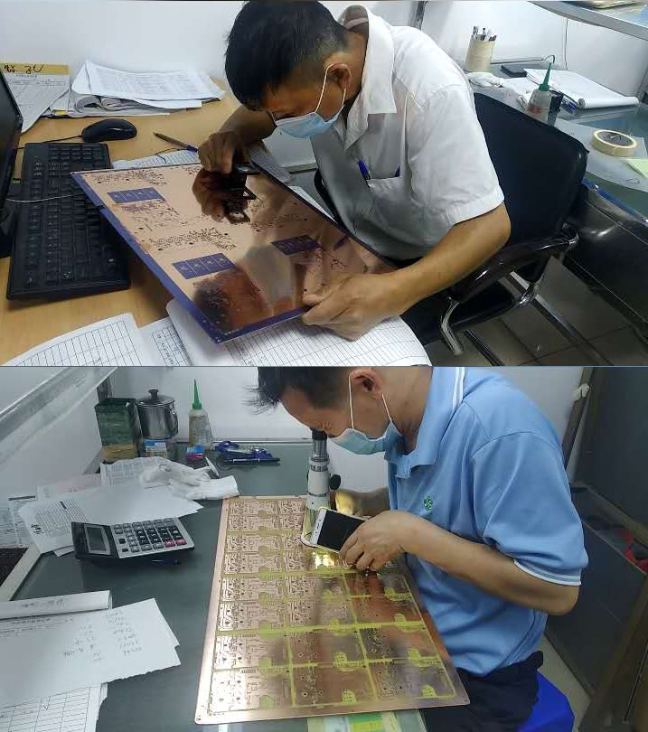
Our manufacturing and assembly hubs in Southern China leverage a complete electronics supply chain to offer cost and logistics advantages for Tokyo-based firms. Because China manages the sourcing of copper-clad laminates (CCL), prepreg sheets, and surface-finishing chemicals locally, we avoid the delays common to fragmented global supply chains.
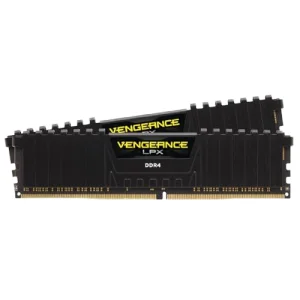
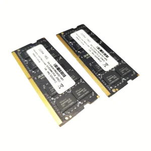
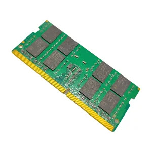
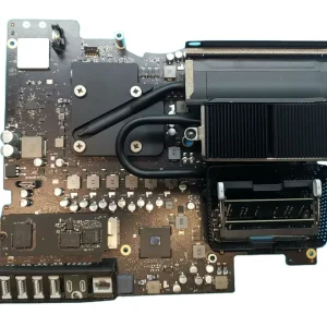
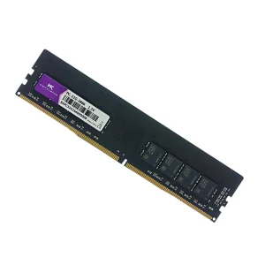
Innovative memory layout, robust packaging, and high-frequency engineering serving high-temperature embedded ecosystems.
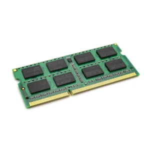
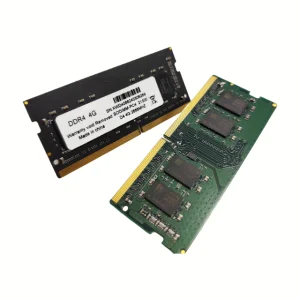
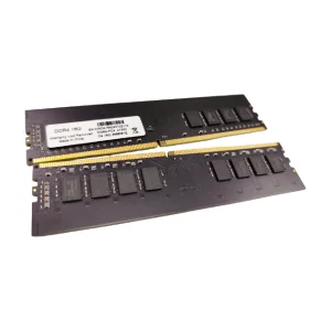
NexaRAM Storage Technology Co., Ltd. is a professional DDR5 memory manufacturer specializing in high-performance RAM solutions for global OEMs, data centers, and enterprise computing applications. Established in 2016, the company has developed into a reliable supplier in the advanced DRAM industry.
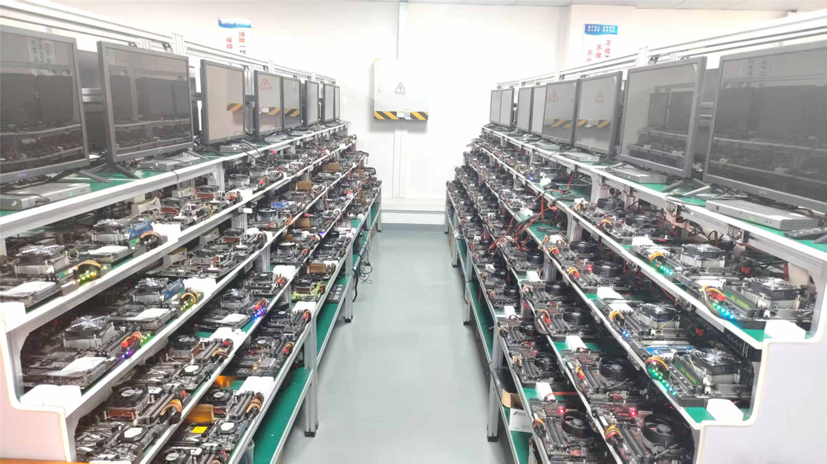
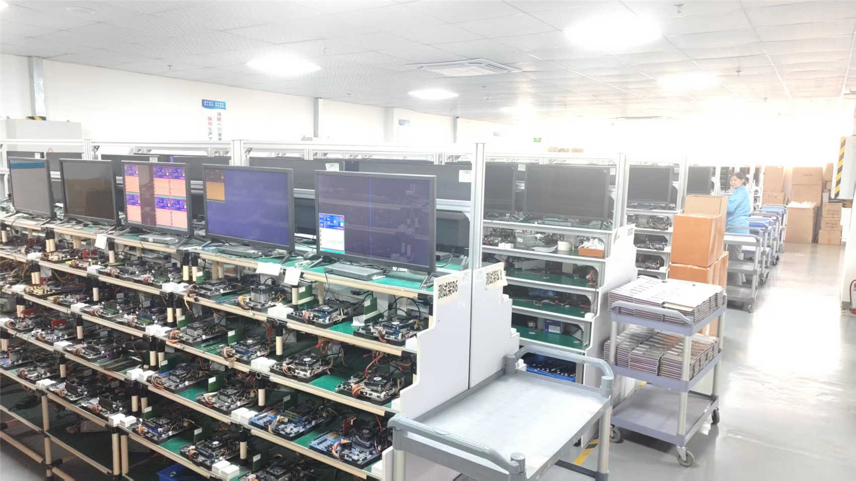
The company operates a modern production facility equipped with advanced manufacturing and testing systems to ensure stable, efficient production capacity. NexaRAM has an annual export revenue of approximately USD 12 million, with 6 years of export experience and 12 years of industry experience in memory and semiconductor-related fields.
Quality is controlled through a combination of automated optical inspection (AOI) and burn-in reliability testing, supported by a professional QC team of 35 inspectors. The company follows international trade compliance standards and operates under a strong global trading background, serving markets across North America, Europe, Southeast Asia, and the Middle East.
NexaRAM maintains a supply chain ecosystem with over 850 strategic supply chain partners, enabling stable sourcing of high-grade semiconductor materials and components. Our primary customer base includes OEM manufacturers, system integrators, server solution providers, and gaming PC brands.
We demonstrate strong R&D capabilities, offering custom DDR5 module design, PCB layout optimization, frequency tuning, and thermal solution development. Flexible customization options include frequency, latency, capacity, heat spreader design, and branding services. In the past year, NexaRAM launched 120 new product variants, supported by a dedicated R&D team of 180 engineers, continuously driving innovation in high-speed memory solutions for next-generation computing systems.


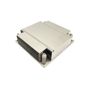
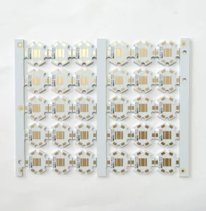
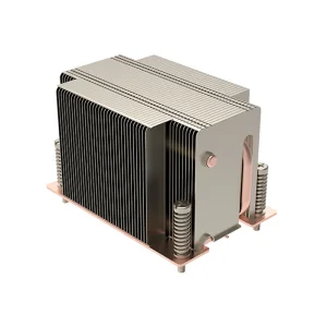
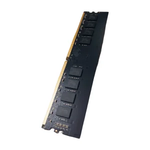
Engineered to withstand prolonged operational temperatures, featuring robust industrial-grade packaging.
In Tokyo's neighboring automotive R&D hubs (such as Yokohama and Toyota City), electronics must withstand demanding under-the-hood conditions. Electronic Control Units (ECUs) and Advanced Driver Assistance Systems (ADAS) operate near high-temperature internal combustion engines or power electronics in electric vehicles. Utilizing High-TG PCBs prevents thermal cycling failures, maintaining electrical performance under vibrations and temperatures up to 150°C.
Tokyo's precision factories rely on continuous automated assembly lines. The robotic controllers, servo drives, and sensor modules on the factory floor generate high heat. High-TG PCBs prevent delamination in multi-layer boards, supporting constant operation and reducing plant downtime.
Outdoor 5G base stations deployed across high-density urban areas like Shinjuku, Shibuya, and Ginza face seasonal weather changes. High-TG materials ensure these boards resist moisture absorption and structural wear, providing stable dielectric constants (Dk) and low dissipation factors (Df) for high-frequency signal paths.
To serve the strict Japanese electronics market, every batch of High-TG PCBs is tested using Automated Optical Inspection (AOI), X-ray structural validation, and flying probe testing. Our base laminates undergo thermal stress testing at 288°C to ensure zero delamination before leaving our facility.
Technical answers to common questions from procurement managers, electronics design engineers, and systems integrators in Japan.