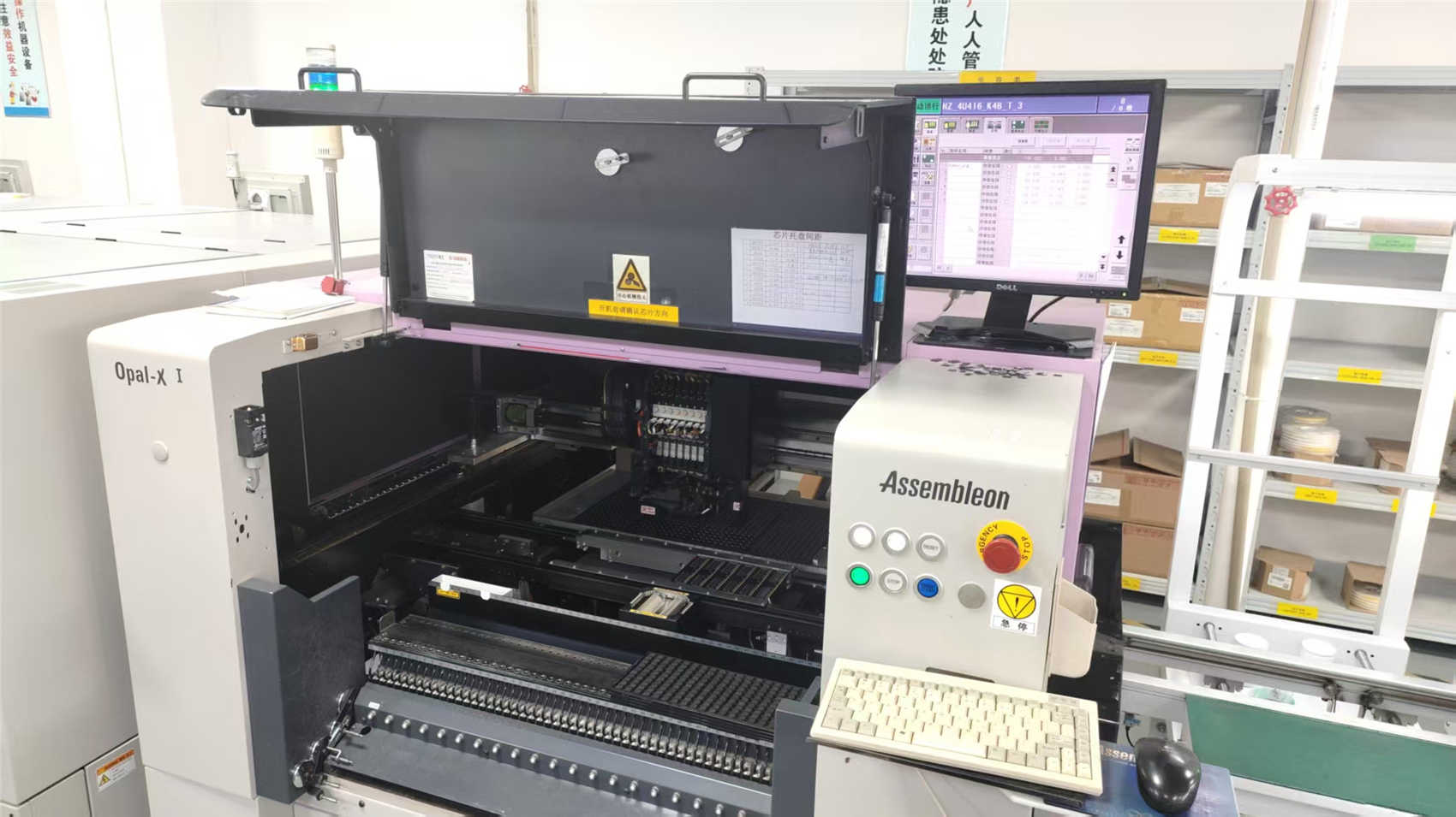
NexaRAM Storage Technology Co., Ltd. stands at the forefront of advanced hardware solutions as a premier manufacturer specializing in high-performance DDR5 memory modules and multi-layer enterprise motherboard architectures. Established in 2016, NexaRAM has expanded its engineering capabilities to supply global OEMs, enterprise data centers, and advanced automation system integrators. Our production infrastructure integrates state-of-the-art SMT (Surface Mount Technology) processes optimized for high-speed, multi-density circuit assemblies.
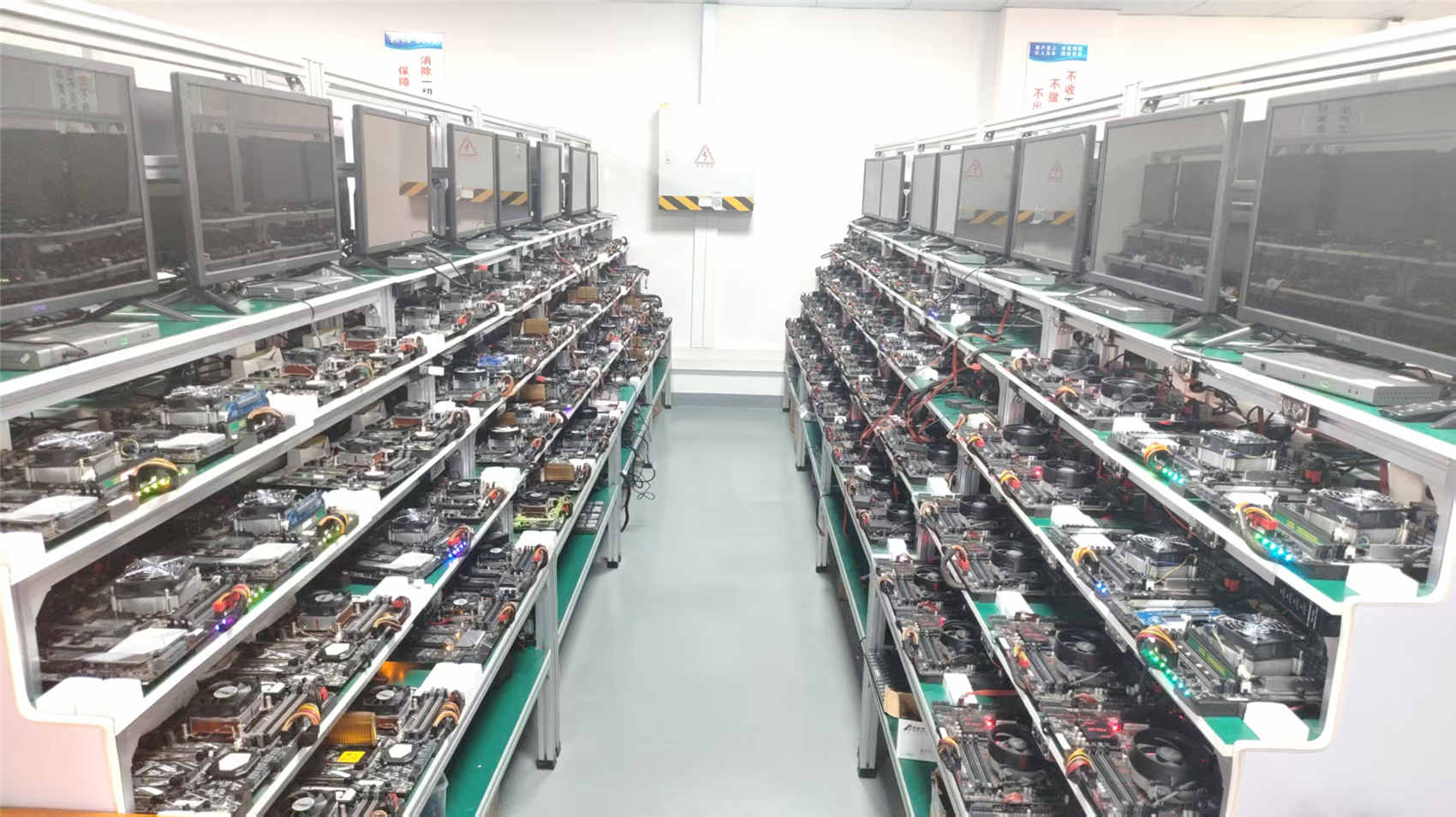
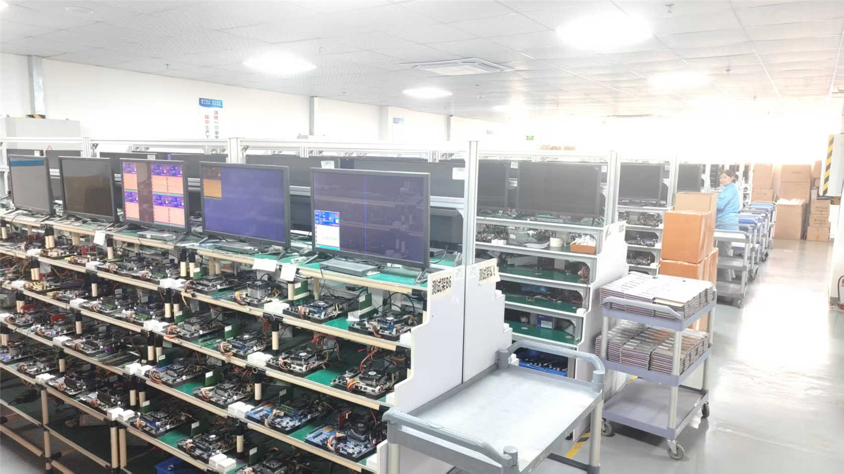
Operating from a specialized cleanroom and production facility spanning 320㎡, NexaRAM combines micro-precision semiconductor assembly with exhaustive testing matrices. This guarantees that every memory circuit board and embedded computing core meets stringent signal integrity and thermal efficiency thresholds. Supported by a rigorous quality system involving 35 dedicated quality inspectors, our processes conform to IPC class standards and ISO-certified manufacturing norms.
With over 6 years of international trade history, our logistics framework spans key industrial markets throughout North America, Europe, Southeast Asia, and the Middle East. We manage end-to-end component traceability, maintaining partnerships with the world's leading semiconductor foundries and passive component manufacturers. This enables us to insulate our production lines from international supply chain volatility and deliver consistent lead times on complex multi-layer PCBA programs.
In the contemporary industrial ecosystem, PCBA procurement has transitioned from simple contract manufacturing to a strategic co-engineering model. Industrial buyers, automotive OEMs, and data center operators require more than standard assembly services. They demand comprehensive supply chain validation, raw material certification, and predictable engineering pipelines.
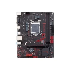
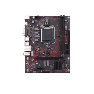
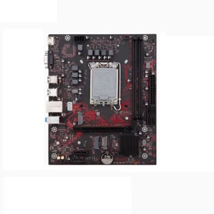
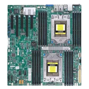
Enterprise infrastructures demand DDR5 layouts, multi-layer server motherboards (supporting PCIe Gen 5/6), and high-frequency PCBs. These configurations mandate impedance controls below ±5% tolerances, ultra-low-loss dielectric laminates (e.g., Rogers, Panasonic Megtron 6), and complex layer stackups designed to mitigate electromagnetic interference (EMI).
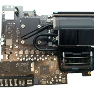
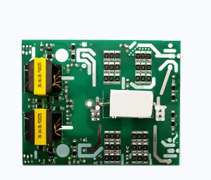
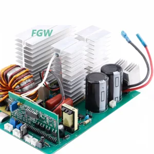
Power supply systems, industrial heavy-duty inverter drives (such as the ZX7 welding driver boards), and automation controllers require heavy copper layers (up to 4 oz or more) to handle elevated currents. Thermal management is critical, relying on custom copper-aluminum composite boards and specialized thermal interface materials (TIMs) to conduct heat away from MOSFETs and power ICs.
Medical monitoring equipment and high-frequency communication transceivers require IPC Class 3 level fabrication. This standard demands zero defect assembly, rigorous component traceability back to primary silicon vendors, and conformal coating to withstand exposure to chemicals, dust, and humidity.
As the digital landscape evolves, modern PCBA manufacturers must align design phases with advanced industrial realities. NexaRAM bridges the gap between hardware conception and volume manufacturing through an array of end-to-end macro solutions:

Before launching full-scale surface mounting, NexaRAM's engineering team executes a deep-dive DFM audit on client Gerber layouts. This process optimizes component spacing, footprint geometries, thermal relief designs, and panelization strategies. By preventing defects such as component skewing or tombstoning during reflow soldering, DFM drastically improves yield rates and lowers production costs for volume runs.
Modern devices require compact footprints and complex multi-layer boards. We offer laser-drilled microvias, blind and buried via layouts, and stacked configurations to maximize routing density across 8 to 24 layers. This approach prevents signal degradation across high-speed channels and supports advanced fine-pitch BGA packaging, including PCIe Gen 5 controller chips and high-frequency memory controllers.
Looking toward the next decade, edge-computing AI devices and high-bandwidth processing units will require advanced PCBA substrates. NexaRAM's technology roadmap targets the integration of next-generation DDR5 configurations capable of operating at transfer rates beyond 6400 MT/s, alongside initial R&D for DDR6-class module footprints. Additionally, we are pioneering the implementation of copper-aluminum composite heat spreaders. This technology enables rapid thermal dissolution, preserving signal fidelity and preventing localized component degradation.
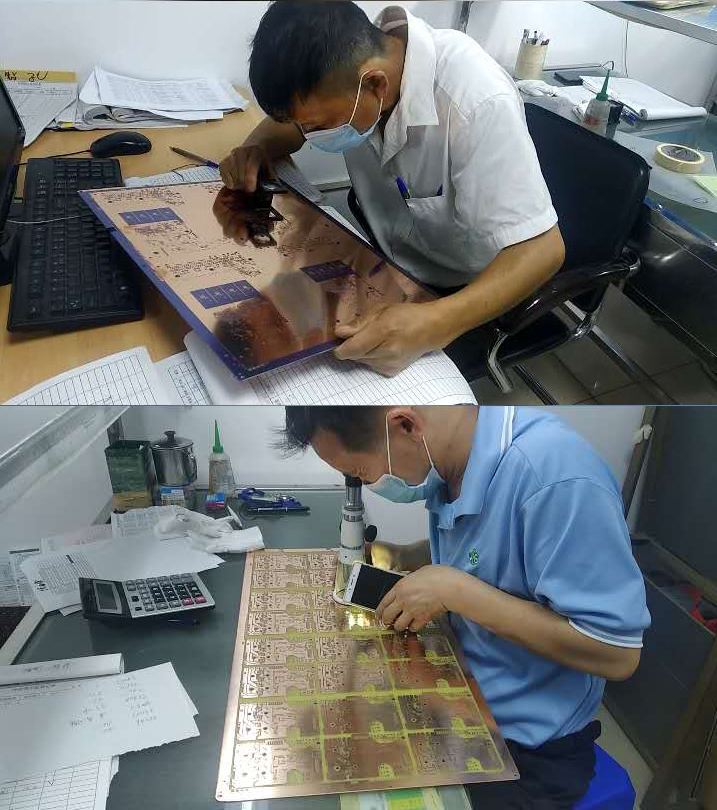
At NexaRAM, quality assurance is an active process embedded in every step of the manufacturing cycle. To achieve high yields and support long-term product lifecycles, our facilities utilize a range of specialized optical, electronic, and thermal validation protocols:


Exporting high-technology assemblies worldwide requires strict adherence to international trade guidelines, safety certificates, and material compliance systems. NexaRAM provides a fully integrated international trade framework that streamlines logistics and minimizes customs delays:
All PCBA products fabricated by NexaRAM comply with global ecological mandates, including RoHS 3 (Restriction of Hazardous Substances) and REACH (Registration, Evaluation, Authorization and Restriction of Chemicals). We maintain clear documentation for lead-free solder processes and use fire-retardant substrates that meet UL 94V-0 flammability standards.
With 6 years of dedicated export experience, our team coordinates customs clearance, tariff classifications, and international shipping protocols. We support multiple shipping terms (including FOB, CIF, EXW, and DDP) to simplify procurement for purchasing agents worldwide.
We offer engineering support across different time zones to assist with layout adjustments, component substitution, and post-delivery troubleshooting. Additionally, our structured RMA (Return Merchandise Authorization) process provides quick replacements or modifications if issues arise in the field.
To assist procurement managers, systems engineers, and supply chain directors, we have compiled detailed answers addressing the primary challenges in high-frequency motherboard and memory module sourcing:
DDR5 memory modules operate with much higher data rates and lower signal margins than prior generations. To maintain signal integrity, NexaRAM's design team utilizes advanced simulation software to evaluate track reflections, crosstalk, and power delivery network (PDN) stability. We place the Power Management IC (PMIC) directly on the memory module to improve power regulation, and design multi-layer stackups with dedicated return paths. This keeps electromagnetic interference (EMI) and signal distortion to a minimum.
Yes. Our engineering division (comprising 180 design engineers) specializes in custom layouts for high-density applications. We can tailor the PCB dimensions, layer stackups, connector styles, and thermal configurations to meet your specific requirements. We also offer frequency tuning and latency matching to optimize module performance for specialized computing platforms, industrial PCs, and custom network hardware.
Component authenticity is a key focus of our quality system. We source semiconductor packages, DRAM silicon, and passive components directly from authorized distributors or the manufacturers themselves. Every production run is tracked using an internal ERP system. This system links each batch of PCBs to the raw material shipments, solder paste batches, and specific SMT lines used during assembly. This allows for full component traceability if verification is ever required.
Heavy-duty industrial electronics (such as the ZX7-200/250 and ZX7-315 driver boards) are subject to high voltages and mechanical vibration. We test these assemblies using high-current test fixtures, functional simulation, and thermal burn-in. We also verify the thickness and coverage of conformal coatings to protect the boards from dust, moisture, and chemical exposure in harsh operational environments.
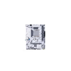
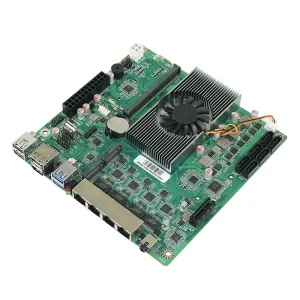
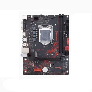
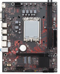
Compact designs (like our N100 and N5095 mini-ITX boards) put components in close proximity, which can lead to heat concentration. We address this by using thick copper planes (up to 2 oz) for improved thermal distribution. We also design dedicated thermal vias and use copper-aluminum composite heatsinks. This keeps junction temperatures for processors, memory components, and power circuits within safe operating limits under continuous load.
For custom projects, layout design and DFM analysis typically take 7 to 14 working days. Once the layout is approved, we can fabricate prototypes in 5 to 7 days. Standard volume production takes between 15 and 25 working days, depending on component availability and the complexity of the assembly. Our strategic supply chain partnerships help keep lead times stable, even during periods of high market demand.