Explore our industrial high-frequency circuit boards, computing modules, and thermal dissipation systems designed for 24/7 heavy-duty operations.
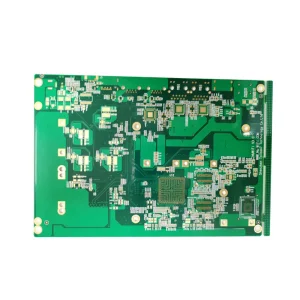
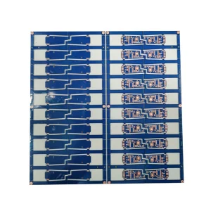
Modern telecommunications, edge AI acceleration, high-frequency computing, and industrial-grade power electronics are shifting towards complex high-density printed circuits. Multi-layer PCBs (typically containing 4 to 32+ conductive copper layers interleaved with specialized dielectric prepregs) form the hardware foundation of this evolution. Standard double-sided boards no longer suffice to suppress signal attenuation, mitigate electromagnetic interference (EMI), and maintain power distribution efficiency under high frequencies.
Integrating complex Multi-layer circuits requires an in-depth understanding of layer stack-up optimization, copper balancing, and thermal coefficient of expansion (TCE) matching. Without precise layout symmetry, asymmetric stress during standard wave soldering or high-temperature reflow cycles causes PCB warpage, fracturing fine-pitch microvias and leading to premature field failure.
Achieving superior signal integrity and ruggedness through selective materials, laser micro-drilling, and controlled impedance profiles.
From standard high-Tg FR-4 (Tg ≥ 170°C) to low-loss hydrocarbon ceramics and PTFE laminates (e.g., Rogers, Megtron series). Proper selection minimizes dissipation factors (Df) and dielectric constants (Dk) at high-frequency ranges up to 77GHz.
Implementing laser-drilled blind and buried microvias (stacked or staggered configurations) enables reliable layer transitions down to 0.1mm diameters, freeing up vital lateral routing space for ultra-fine pitch BGAs.
Utilizing high-precision automated etching lines to guarantee differential line impedance deviations within ±5% (or even ±3% for custom high-speed applications like high-capacity servers and telecom equipment).
NexaRAM Storage Technology Co., Ltd. leverage a dense local network to ensure high efficiency, stable raw material access, and rapid volume scaling.
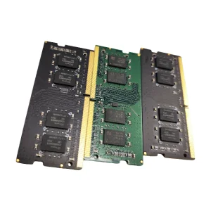
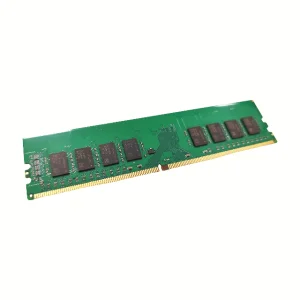
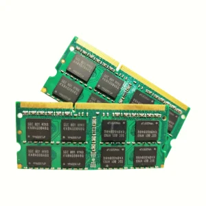
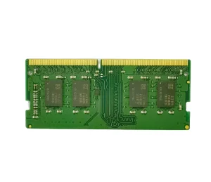
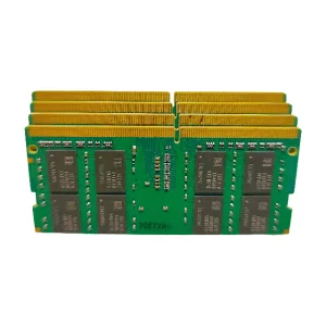
NexaRAM Storage Technology Co., Ltd., founded in 2016, serves as a high-performance DRAM memory module manufacturer and advanced subsystem assembly partner. Headquartered in a dedicated 320㎡ cleanroom testing facility, NexaRAM specializes in high-speed, high-density surface mount technology (SMT) and semiconductor module integration. With over 12 years of industry experience and 6 years of export history, we generate an annual export volume of approximately USD 12 million.
Our operations rely on an expansive supply chain, containing over 850 strategic partners. This structure ensures a steady supply of top-tier materials: from copper clad laminates (CCL) and chemical reagents to grade-A DRAM chips and high-performance server thermal components. By combining localized manufacturing clusters with stringent quality systems, we achieve unmatched prototyping speed and seamless high-volume scaling.

Where high-density multi-layer boards and high-frequency modules are deployed across global industries.
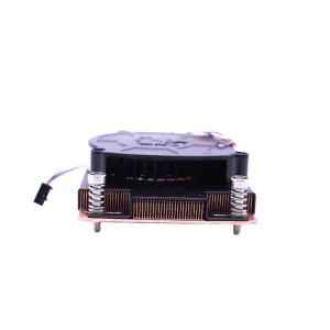
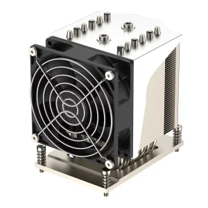
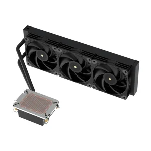
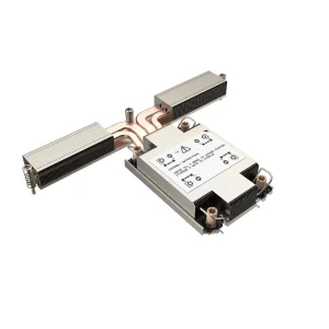
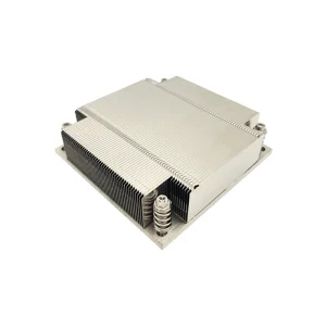
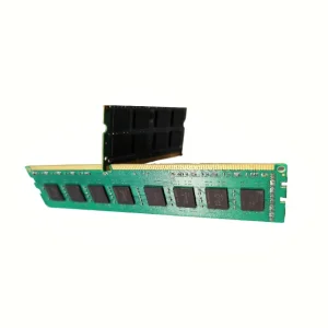
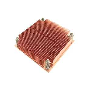
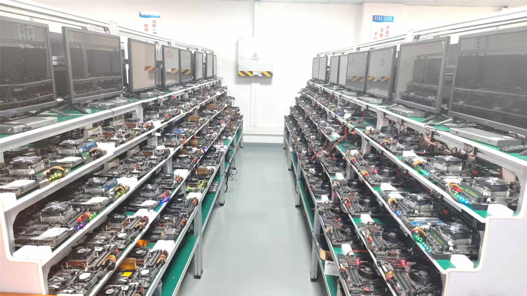
Powering 1U/2U/4U enterprise-grade servers requiring high-speed PCB layouts, DDR4/DDR5 memory integration, and passive/active LGA4677/SP3 copper cooling modules.
Utilized in heavy-duty welding systems, power banks, and high-frequency inverters where heavy copper traces (up to 4oz or 6oz) are required to carry high currents.
Enabling base stations, routers, and high-speed switches with specialized multi-layer stack-ups that keep signal loss to a minimum at microwave frequencies.
Supporting advanced driver assistance systems (ADAS) and power management controllers that demand zero-defect tolerance (IPC Class 3 reliability standards).
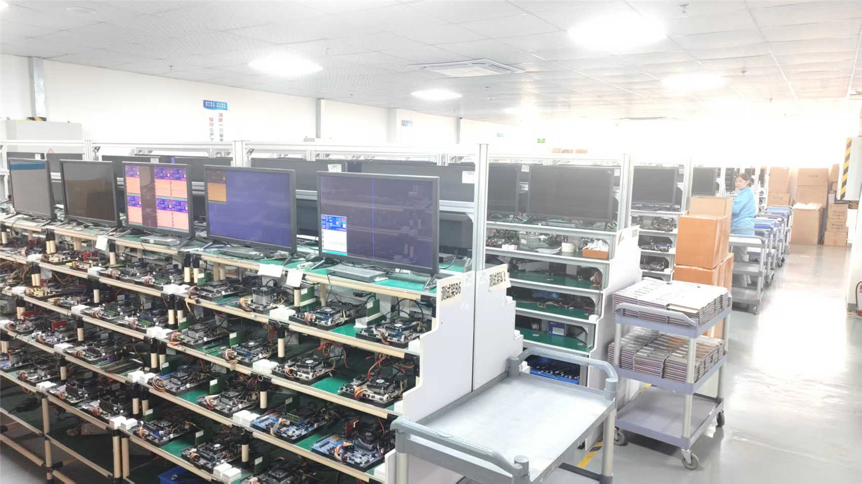
Every batch of Multi-layer boards and memory modules undergoes comprehensive optical and electrical validation before export.


Exporting high-precision PCBs and memory components to North America, Europe, Southeast Asia, and the Middle East demands strict alignment with complex regulatory frameworks. NexaRAM strictly adheres to RoHS, REACH, CE, and FCC guidelines, guaranteeing that all raw laminates, copper-clad boards, solder-resists, and active chips are free of restricted hazardous substances.
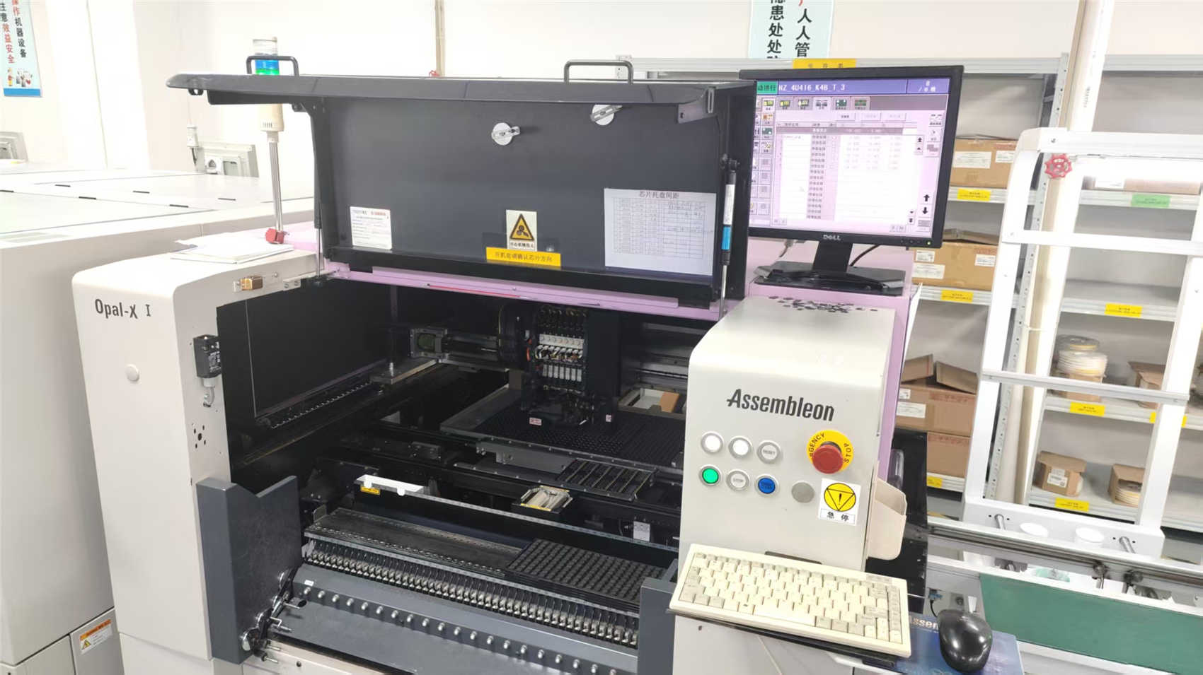
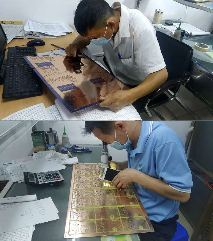
Our quality control infrastructure combines Automated Optical Inspection (AOI) to trace structural micro-flaws, 3D X-ray (AXI) to inspect inner-layer registration and buried solder joint integrity, and 100% functional burn-in tests. This system guarantees that every PCB assembly and DRAM memory unit maintains operational stability under extreme thermal cycling and high-frequency workloads.
Common questions concerning multi-layer PCB design specifications, thermal management, production times, and shipping logistics.
Prototyping multi-layer PCBs (from 4 to 8 layers) typically takes 3 to 5 working days, depending on stacking complexity and microvia requirements. Mass-production runs range between 10 to 18 working days, including time for automated tooling setup, optical testing, and QA inspections.
We define track width and clearance dimensions using software models such as Polar Instruments. We track etching tolerances with AOI and use specialized time-domain reflectometry (TDR) to test impedance, keeping line impedance tolerance within ±5%.
Yes, our team of 180 engineers provides custom DDR5 module design, PCB layout optimization, frequency tuning, and thermal analysis. We optimize trace routing and heat-sink contact areas, and integrate thermal vias to enhance heat dissipation.
We process high-Tg laminates such as Isola, Shengyi, and Rogers PTFE for radar/ADAS. This ensures optimal thermal resistance and keeps thermal expansion coefficients (CTE) low across changing temperatures.
Every production lot undergoes SMT solder paste inspection (SPI), Automated Optical Inspection (AOI), and X-ray analysis for BGA voids. Memory modules undergo functional testing using specialized test jigs and high-temperature burn-in cycles.
By working with over 850 strategic partners, we secure multiple sourcing paths for our primary materials. We maintain buffer stocks of essential raw components, ensuring stable manufacturing cycles even during market shortages.
Select specialized equipment, server coolers, adapters, and memory modules for heavy computational workloads.