Engineered for high-yield Surface Mount Technology (SMT) lines. Featuring precise apertures and superior paste-release parameters.
An in-depth study of high-precision micro-aperture engineering, paste-release physics, and local supply chain optimization for Jabodetabek's high-tech manufacturing sector.
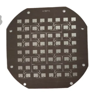
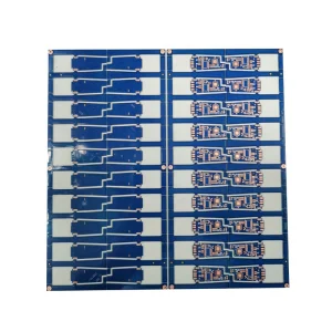
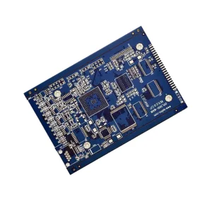
Surface Mount Technology (SMT) is the backbone of modern electronics assembly. At the center of this process is the laser stencil, a high-precision stainless steel foil designed to deposit precise amounts of solder paste onto printed circuit boards (PCBs). The accuracy of this process directly determines the yield and reliability of the final assembly.
For high-density packages such as 01005 passives, micro-BGAs, and fine-pitch QFNs, standard etching techniques are insufficient. Fiber laser cutting technology has emerged as the industry standard, utilizing state-of-the-art multi-axis CNC laser machines to achieve sub-micron dimensional tolerances. Our stencils leverage customized fiber lasers to produce smooth aperture walls with a taper angle typically between 1 to 2 degrees. This positive taper facilitates superior solder paste release, mitigating common defect modes like solder bridging, voids, and insufficient solder volume.
Furthermore, we employ specialized fine-grain (FG) stainless steel foils (such as SUS304 or similar high-tensile alloys) which offer exceptional dimensional stability, reducing aperture distortion under continuous squeegee pressure. This is critical for high-throughput Jakarta-based electronics manufacturing service (EMS) lines operating 24/7.
[Area of Aperture Opening / Area of Aperture Walls].Jakarta, along with the surrounding Jabodetabek region (including Cikarang, Karawang, and Bekasi), stands as the premier hub for Indonesia's industrial transformation under the "Making Indonesia 4.0" roadmap. The region hosts a dense concentration of multinational automotive assembly lines, consumer electronics manufacturers, and telecommunications equipment providers.
The transition toward electric vehicles (EVs), smart grid infrastructure, and localized IoT device fabrication has triggered a surging demand for localized, rapid-turnaround SMT tooling. Automotive Engine Control Units (ECUs), LED lighting modules, and advanced battery management systems (BMS) require high-precision PCBs with thick copper layers or specialized high-frequency substrates. To support these local assembly lines, high-performance laser stencils are critical for ensuring zero-defect soldering on safety-critical assemblies.
Additionally, Jakarta's proximity to Soekarno-Hatta International Airport and major sea shipping lanes enables integrated logistics routes that bridge Chinese advanced fabrication centers with local Indonesian factories. This hybrid ecosystem combines local customer service and rapid prototyping with the vast capacity and supply chain resilience of Chinese manufacturing.
Indonesia's electronic production volume is projected to grow significantly. SMT assembly capacity in Java's industrial zones is expanding to capture shifting global supply chains. Key demands include:
Chinese high-tech fabrication complexes leverage unmatched supply chain density. By consolidating raw material sourcing (SUS304/FG foils, raw polymer frames), automated laser-cutting stations, and digital quality control pipelines, we guarantee both cost-efficiency and technical consistency.
Our integrated software pipeline performs automated DFM (Design for Manufacturability) checks on stencil aperture files within minutes of submission. The automated CNC laser stations execute paths optimized by AI algorithms, minimizing heat-affected zones (HAZ) and ensuring perfect fidelity to customer Gerber data.
Global procurement directors face a complex balancing act: minimizing unit costs while ensuring maximum product reliability. In SMT assembly, a low-quality stencil can lead to high defect rates (such as solder balling or bridging), causing expensive rework cycles or field failures. Procuring high-end laser stencils from advanced factories in China offers a competitive edge, combining competitive pricing with state-of-the-art precision.
By partnering with a manufacturer that adheres to international IPC-7525B standards, procurement teams in Jakarta can confidently secure stencils that integrate seamlessly with high-speed printing platforms like DEK, MPM, or Yamaha. Furthermore, the combination of advanced laser cutting and automated optical inspection (AOI) guarantees 100% aperture conformance prior to dispatch, eliminating incoming quality control (IQC) bottlenecks at the customer's facility.
From the industrial estates of Karawang to the tech-parks of Tangerang, our products support critical electronics assembly applications.
Modern vehicles require high-power electronic components to manage everything from drivetrains to advanced driver-assistance systems (ADAS). These components rely on heavy copper PCBs and ceramic substrates designed to dissipate substantial heat. Our high-precision laser-cut stencils ensure uniform solder paste deposition, minimizing voiding under large thermal pads and maintaining robust solder joint integrity under high-vibration conditions.
The roll-out of 5G infrastructure throughout Jakarta requires dense RF boards utilizing high-frequency materials like Taconic and Rogers. Standard stencils struggle to deliver the precise volumes of solder paste needed for high-frequency shielding cans and micro-fine pitch transceivers. We offer specialized step-down stencils with customized thickness profiles to accommodate mixed-component assemblies on a single board.
Indonesia's ongoing updates to utility grids require localized production of smart water, gas, and electricity meters. These high-volume assemblies need extremely reliable SMT tooling to keep assembly costs low. Our laser-cut stencils are optimized for durability, supporting high print cycles with minimal downtime for cleaning or maintenance.
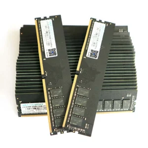
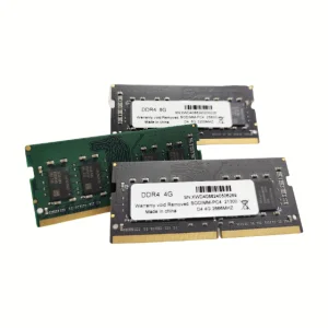
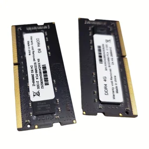
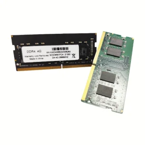
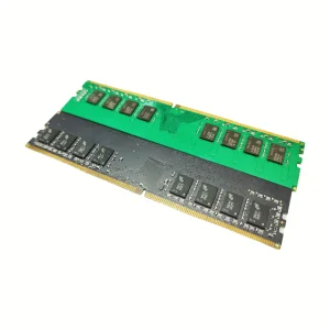
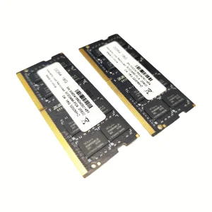
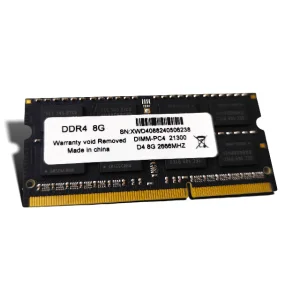
Advanced enterprise computing relies on high-speed DRAM and solid-state storage. We support memory module assembly with precision stencils designed for BGA packages down to 0.4mm pitch. This expertise in micro-precision tooling is backed by our parent semiconductor division, NexaRAM Storage Technology.
Combining years of industry experience with state-of-the-art testing and QA equipment to deliver premium industrial solutions.
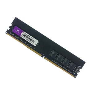
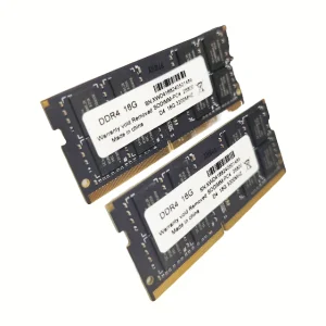
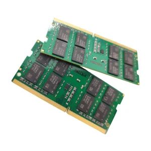
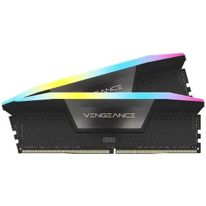
NexaRAM Storage Technology Co., Ltd. is a professional DDR5 memory manufacturer specializing in high-performance RAM solutions for global OEMs, data centers, and enterprise computing applications. Established in 2016, the company has rapidly developed into a reliable supplier in the advanced DRAM industry.
The company operates a modern production facility with a total building area of approximately 320㎡, equipped with advanced manufacturing and testing equipment to ensure stable and efficient production capacity. NexaRAM has an annual export revenue of approximately USD 12 million, with 6 years of export experience and 12 years of industry experience in memory and semiconductor-related fields.
Quality is strictly controlled through a combination of automated optical inspection (AOI) and burn-in reliability testing, supported by a professional QC team of 35 inspectors. The company follows international trade compliance standards and operates under a strong global trading background, serving markets across North America, Europe, Southeast Asia, and the Middle East.
NexaRAM maintains a highly developed supply chain ecosystem with over 850 strategic supply chain partners, enabling stable sourcing of high-grade semiconductor materials and components. Its primary customer base includes OEM manufacturers, system integrators, server solution providers, and gaming PC brands.
The company demonstrates strong R&D capabilities, offering custom DDR5 module design, PCB layout optimization, frequency tuning, and thermal solution development. Flexible customization options include frequency, latency, capacity, heat spreader design, and branding services.
In the past year, NexaRAM launched 120 new product variants, supported by a dedicated R&D team of 180 engineers, continuously driving innovation in high-speed memory solutions for next-generation computing systems.


Direct technical answers addressing common inquiries from process engineers and procurement directors in the Jakarta electronic manufacturing corridor.
Fine-grain (FG) stainless steel has a much smaller grain structure (typically 1 to 5 microns) compared to standard SUS304 steel (typically 15 to 25 microns). This micro-level structure allows for smoother aperture walls after laser cutting, resulting in a cleaner edge profile. In practice, FG foils improve paste release for ultra-fine-pitch components (such as 0.4mm pitch BGAs) and help maintain stencil tension, extending the tool's operating life on high-volume SMT lines.
For fine-pitch micro-BGAs, we adhere to the IPC-7525B standard, targeting an area ratio (AR) of 0.66 or higher. The formula is AR = D / 4H (where D is the aperture width/diameter and H is the stencil foil thickness). When the required pitch drops and the AR falls below 0.66, we recommend reducing the foil thickness or applying a hydrophobic nano-coating. This coating modifies the surface tension on the aperture walls, enabling consistent paste release even at lower area ratios.
Step-up and step-down stencils are used when components with different solder volume requirements are placed on the same PCB. Step-up zones increase stencil thickness in areas requiring larger solder volumes (e.g., connectors or power inductors), while step-down zones reduce thickness for fine-pitch components (e.g., QFNs or micro-BGAs). The transition slope must be calculated to prevent the squeegee from hovering over low spots. We maintain a standard slope ratio of 1:40 (thickness difference to transition length) to ensure clean squeegee travel across the stencil.
To prevent warp or distortion during shipping, all stencils are mounted under tension on rigid aluminum frames using heavy-duty epoxy adhesives. We package each unit with thick, shock-absorbing foam layers inside reinforced, moisture-resistant shipping boxes. In addition, we coordinate with major express couriers to minimize transit time to Soekarno-Hatta Airport (typically 3-4 working days) and protect the stencils from extreme environmental changes.
Hydrophobic and flux-phobic nano-coatings repel both flux and solder paste. This prevents paste from adhering to the underside of the stencil during the printing cycle. As a result, the stencil requires less frequent cleaning cycles (often extending from every 3-5 prints to every 20-30 prints), reducing cleaning solvent consumption and minimizing print-related defects like bridging and solder balls.
Yes. Our engineering team conducts design-for-manufacturability (DFM) reviews on all incoming Gerber files. To mitigate solder balling on passive components (like 0603 or 0805 packages), we can apply home-plate, bow-tie, or inverted-home-plate aperture shapes. These designs reduce the volume of solder paste deposited under the center of the component body, preventing paste squeeze-out and subsequent solder ball formation.
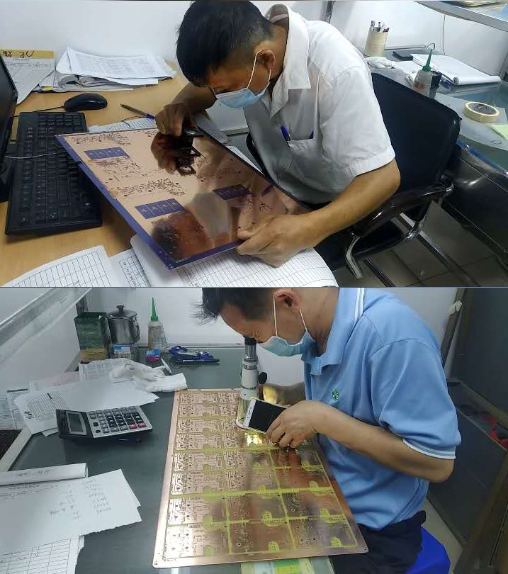
We verify every stencil using an automated optical inspection (AOI) system dedicated to stencil inspection. The AOI compares the cut stencil against the original Gerber data to verify aperture position, size, and wall quality. This process detects issues like incomplete cuts or dimensional drift. A detailed inspection report is provided with every shipment to ensure traceablity and quality control.
Our standard manufacturing lead time is 24 hours from engineering approval of the Gerber files. Shipping via international express to Jakarta's main industrial estates typically takes 3 to 4 business days. This allows us to deliver high-precision stencils to your facility within 5 business days, providing a reliable option for both prototype runs and production lines.
For RF shield cans, we design step-up stencils or use localized aperture expansion to deposit a sufficient volume of solder paste on the shield's perimeter. We also design relief pockets on the squeegee side if the shield must be printed over pre-placed components, ensuring uniform paste deposition without disturbing existing parts.
We recommend cleaning stencils with specialized, pH-neutral SMT cleaning agents or isopropyl alcohol (IPA) using lint-free wipes. Avoid using abrasive brushes or harsh chemicals, which can damage nano-coatings or weaken the tension mesh. Regular, gentle cleaning helps prevent paste buildup in fine-pitch apertures, ensuring consistent print quality over the life of the stencil.
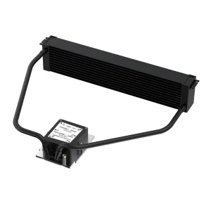
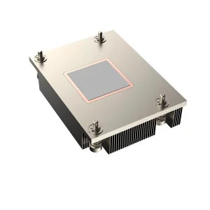
Enterprise-grade DRAM, server heat sinks, and high-density memory modules optimized for industrial computing applications.
Ensure maximum performance across all compute nodes and systems with our additional storage, memory, and semiconductor solutions.