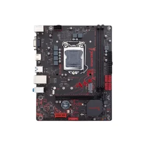
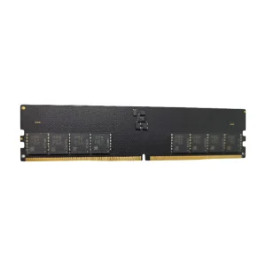
In the era of 5G, 6G, and hyperscale AI computing, the demand for High-Frequency Circuit Boards (HFCB) has skyrocketed. As the nervous system of modern electronics, HFCBs must handle signal frequencies ranging from several GHz to over 100 GHz. Unlike standard FR-4 PCBs, these specialized boards require advanced materials like PTFE (Polytetrafluoroethylene), ceramic-filled hydrocarbons, and proprietary thermoset resins to maintain signal integrity.
Global procurement teams are shifting focus from simple cost-minimization to Total Cost of Ownership (TCO), prioritizing factories that offer thermal stability, low dielectric loss (Df), and tight impedance control. This whitepaper analyzes the current manufacturing landscape and strategic imperatives for sourcing.
The global supply chain for high-frequency electronics is increasingly localized. Leading manufacturers are establishing regional hubs to mitigate geopolitical risks and shipping latency. For enterprise procurement, the vetting process for a factory has evolved:
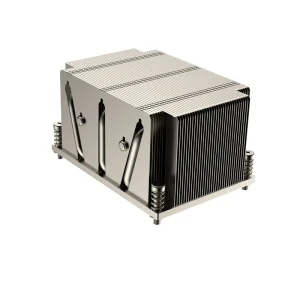
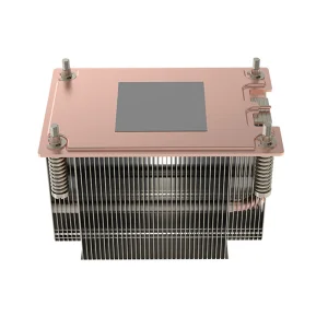
Looking toward 2030, the technology roadmap for HFCBs is converging on three pillars: Thermal Management, Miniaturization, and System-in-Package (SiP) Integration. As AI accelerators become more compact and power-hungry, the integration of thermally conductive PCB substrates with advanced heat dissipation layers is no longer optional—it is essential.
Future Trends:
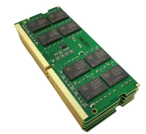
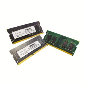
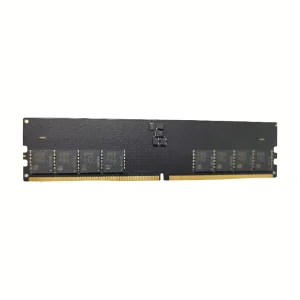
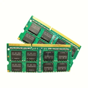
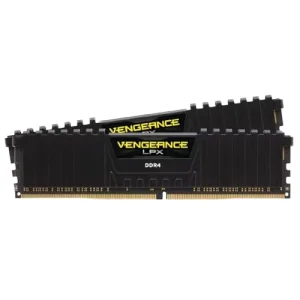
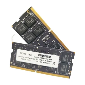
NexaRAM Storage Technology Co., Ltd. stands at the intersection of high-speed memory modules and complex electronic integration. Established in 2016, our journey from DRAM experts to comprehensive system component providers reflects our commitment to the high-frequency requirements of modern computing.
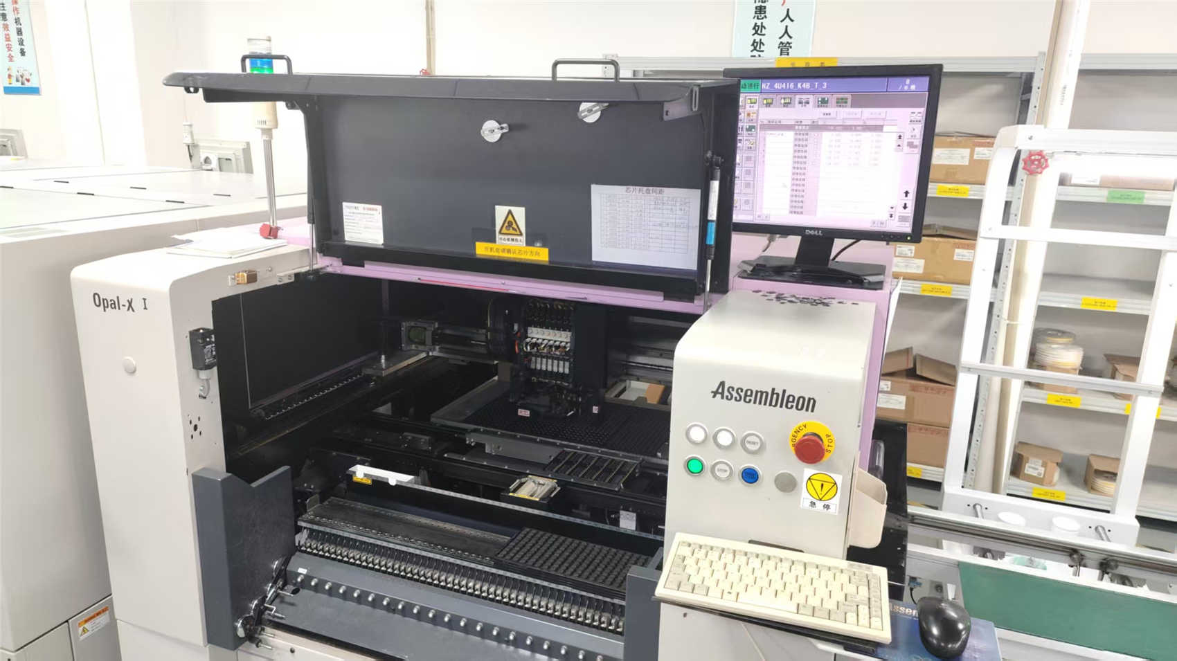
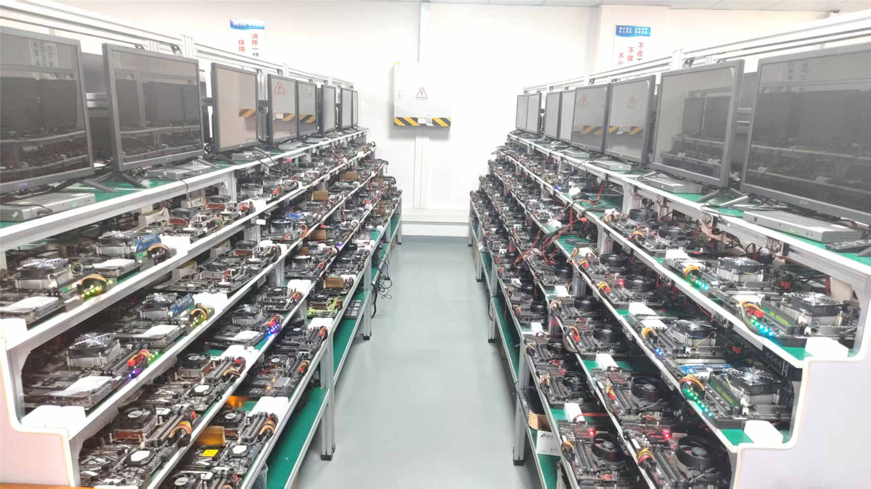
With 12 years of industry experience and a rigorous quality control framework involving 35 dedicated inspectors, NexaRAM leverages automated optical inspection (AOI) and burn-in reliability testing to ensure every component meets the strictest standards for enterprise applications. Serving North America, Europe, and the Middle East, we provide not just memory, but the signal integrity solutions that high-frequency circuit environments demand.
Our R&D team of 180 engineers is constantly pushing the boundaries of frequency tuning, PCB layout optimization, and thermal engineering, ensuring our partners remain ahead of the technological curve.
A: At high frequencies, signals travel on the surface of the conductor. The dielectric constant (Dk) and loss tangent (Df) of the substrate directly impact signal attenuation. Using the wrong material results in massive signal loss and phase distortion.
A: We utilize advanced AOI (Automated Optical Inspection) and rigorous burn-in testing to ensure every module, from memory to integrated systems, maintains optimal signal integrity under high thermal and electrical loads.
A: Yes. Our R&D team specializes in frequency tuning, PCB layout optimization, and thermal solution development, allowing us to customize designs based on specific impedance and application needs.