OEM High-Performance Memory Modules and Cooling Systems
An Industry Whitepaper on Signal Integrity, Advanced Laminates, and High-Performance Compute Infrastructure
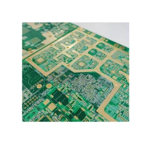
In the era of hyper-scale datacenters, high-frequency enterprise networks, and generative AI computing, hardware performance is bounded directly by electromagnetic physics. As signal rise times shrink to the picosecond scale, the printed circuit board (PCB) evolves from a passive component carrier into an active component in its own right. Understanding the subtle dynamics of Multilayer PCBs, material properties, and layer stackup architectures is paramount for global OEMs and procurement officers demanding uninterrupted performance and high yield rates.
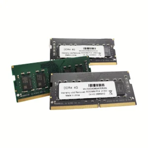
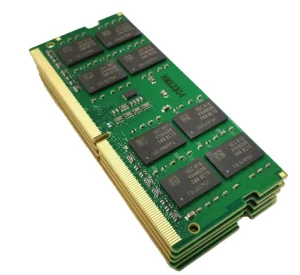
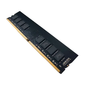
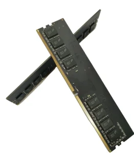
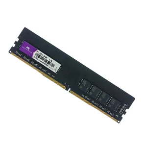
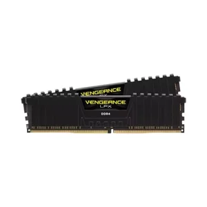
NexaRAM Storage Technology Co., Ltd. (established in 2016, with 12 years of industry experience) stands at the intersection of high-density DRAM integration and complex multilayer PCB design. Delivering state-of-the-art DDR5 memory solutions operating at speeds of 5600MHz and beyond requires a deep mastery of high-frequency, multi-layered substratum physics. In this whitepaper, we dissect the manufacturing paradigms, material science, and strategic supply chain protocols that enable high-reliability signal routing across highly dense multilayer networks.
Maximizing Transmission Performance and Thermal Dissipation across Critical Computing Environments
Utilizing high-end Rogers 4000 series, Shengyi FR4 High TG170, and mixed-dielectric lamination technology. These materials offer low dissipation factors (Df < 0.003) and highly stable dielectric constants (Dk) across varying frequencies up to 40 GHz, minimizing signal attenuation and dispersion in high-speed datacenters.
Incorporating blind and buried vias, stacked microvias, and via-in-pad plating. This optimization reduces parasitic capacitance and inductance, providing a clean impedance path for complex DDR5 BGA packages and multi-gigabit routing environments where structural tolerances are measured in microns.
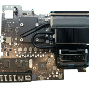
Heavy copper layers up to 6oz, specialized thermal vias, and copper coins are integrated directly within the board structure. This ensures highly efficient heat conduction away from hot silicon, such as CPUs, power management ICs (PMICs), and high-frequency memory controllers, protecting long-term reliability.
Navigating the Transition towards PCIe Gen 6/7, DDR5/DDR6, and High-Speed Optical Integration
As the high-performance computing landscape reaches the physical limits of traditional copper-clad laminates, NexaRAM's R&D engineering team (composed of 180 expert engineers) is actively piloting tomorrow's interconnect systems. The industry is currently transitioning from PCIe 5.0 to PCIe 6.0 and 7.0, where PAM4 signaling requires double the signal-to-noise ratio. To withstand these strict requirements, our multilayer PCB roadmap features several key initiatives:
By coordinating custom design parameters, NexaRAM guarantees seamless electrical and mechanical integration across all hardware layers. This holistic approach ensures that each product variant launched—such as the 120 new variants developed in the past year—functions under optimal thermal and electrical conditions.
Annual Export Revenue (USD)
Dedicated R&D Engineers
Strategic Supply Partners
Years Industry Experience
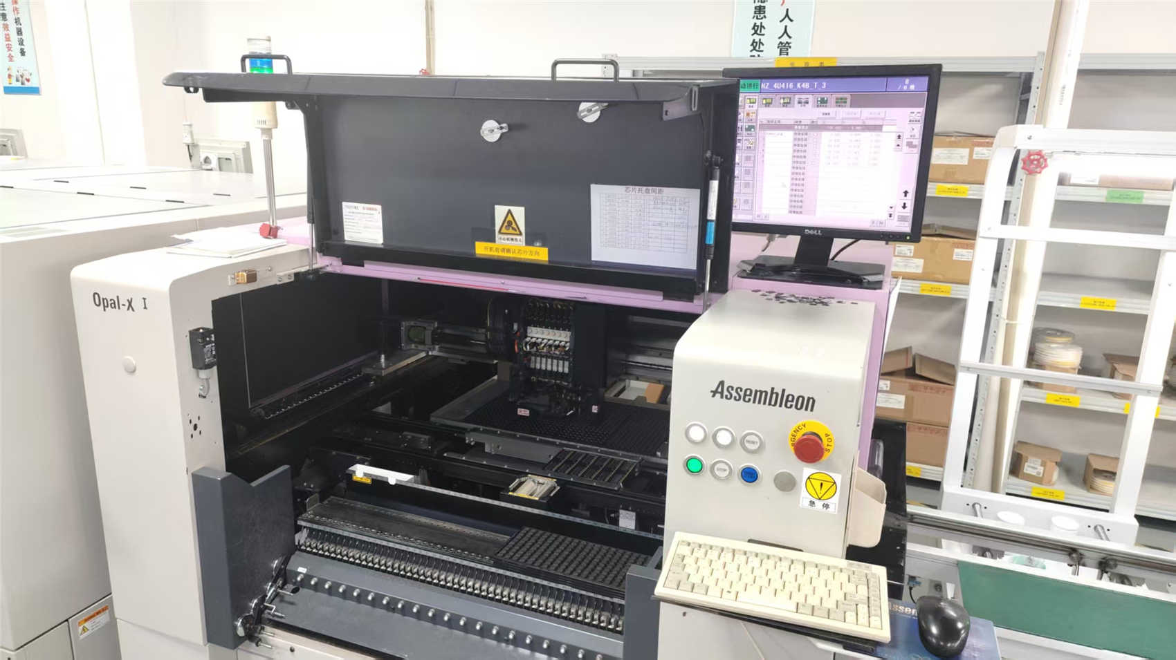
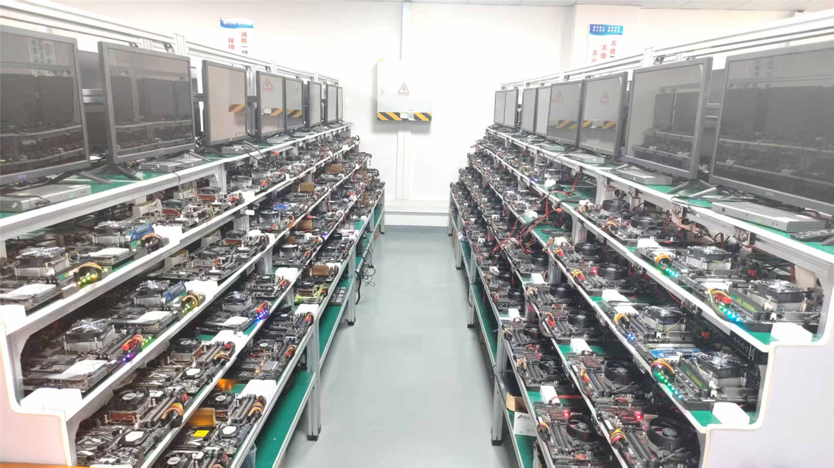
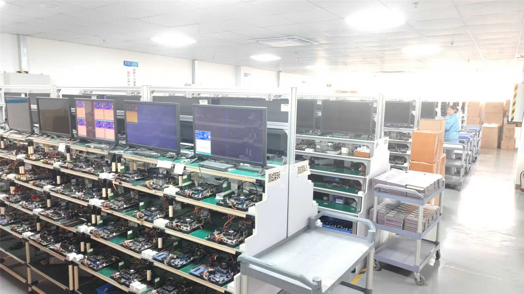
Operating from a specialized modern cleanroom testing facility, NexaRAM leverages a strong manufacturing ecosystem in China to deliver unmatched supply-chain stability and scalability. Quality assurance is built into every layer of our PCB and memory module production process.
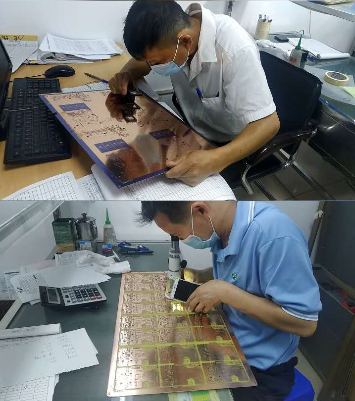
We deploy a multi-stage quality control system overseen by 35 expert inspectors. This system integrates Automated Optical Inspection (AOI), X-ray microscopic verification, and extensive burn-in reliability testing to systematically eliminate micro-faults, cold solder joints, or inner-layer alignment deviations before delivery.
Furthermore, our relationships with over 850 strategic supply chain partners ensure that we secure premium laminate materials (e.g., Rogers, Shengyi, Panasonic Megtron 6) and top-grade DRAM wafers even during periods of global silicon shortage, shielding our global clients from production delays.


Providing Industrial-Grade Systems for Diverse Computing Verticals
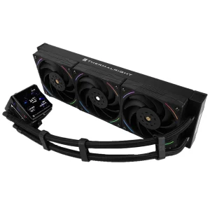
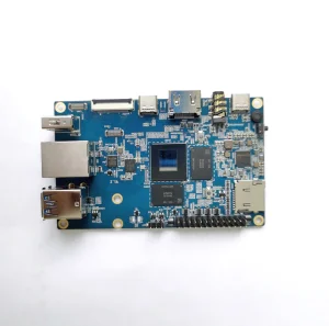
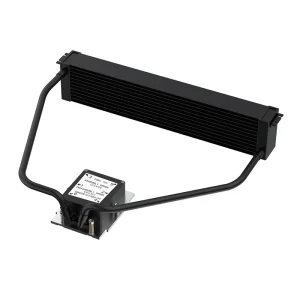
Supporting Next-Gen server architectures with customized high-speed multi-layer backplanes, liquid cooling interfaces, passive SP5 heat sinks, and server-grade ECC memory (DDR4/DDR5) for uninterrupted database access and high virtualization throughput.
Designing custom, temperature-resistant multilayers with low CTE parameters to survive continuous vibration and heat cycles. Ideal for radar systems, autopilot computing units, and sophisticated in-vehicle infotainment.
Ensuring ultra-precise trace geometry and high electromagnetic compatibility (EMC) shielding parameters for imaging systems like MRI, CT, and advanced ultrasonic medical computers.

Global procurement teams face strict regulatory guidelines across international jurisdictions. To ensure total peace of mind, NexaRAM maintains comprehensive certifications: UL 94V-0 flammability ratings, ISO 9001 quality compliance, and RoHS/REACH environmental safety declarations.
Our localized support structure operates across North America, Europe, Southeast Asia, and the Middle East, offering native technical engineering consultations, localized logistics support, and immediate customer service to align with your production runs.
By blending local support with our high-volume Chinese manufacturing base, we offer the optimal balance: Western engineering response times coupled with East Asian manufacturing cost-efficiency and delivery speeds.
Answering High-Level Engineering and Procurement Questions for Enterprise Buyers
We supply and process high-frequency and high-performance laminates from top manufacturers, including Rogers (4000 series, RO4350B, RO4003C), Shengyi (FR4 High TG170 / TG180), Panasonic (Megtron 6), and ITEQ. Our choice of laminate is dictated by target signal speeds, dielectric loss requirements, and thermal dissipation thresholds.
To secure signal integrity at frequencies exceeding 5GHz, we optimize impedance mismatches via precise stackup design. We deploy full electromagnetic wave simulation models (such as HFSS) to analyze trace geometry, minimize crosstalk, balance ground plane loops, and construct blind/buried microvias to eliminate capacitive stubs.
Standard prototyping lead times range from 3 to 7 working days, depending on layer count and complexity. Mass production runs usually require 10 to 18 working days. We also offer expedited quick-turn prototype services for urgent projects, leveraging our advanced supply-chain integration.
We utilize high-resolution lamination presses, laser-direct imaging (LDI), and advanced Automated Optical Inspection (AOI) to verify internal trace layout and spacing. Before final lamination, X-ray inspection is deployed to guarantee accurate vertical interlayer registration down to +/- 0.05mm.
Yes, we specialize in cost-effective hybrid laminations. By using Rogers material exclusively on the outer layer where high-speed RF or digital signals run, and standard FR-4 on internal power and ground layers, we provide the performance benefits of premium substrates at a significantly lower cost.
Every export shipment is fully documented and accompanied by certificates of compliance, including UL 94V-0 ratings, RoHS and REACH declarations, IPC-A-600 Class II or Class III quality reports, and detailed microsection analysis reports upon request.
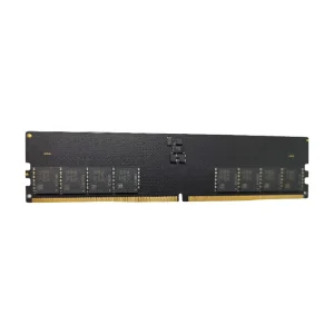
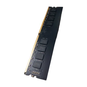
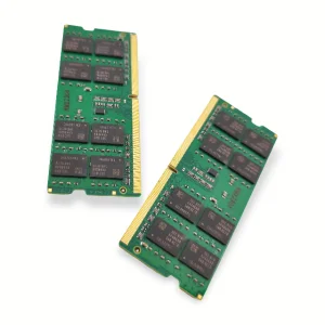
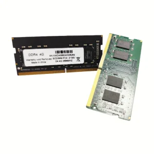
DDR5 Server Kits, High-Performance RAM Modules, and Hydro-dynamic Cooling