1 / 5
| Capability Parameter | Volume Production | Sample Processing |
|---|---|---|
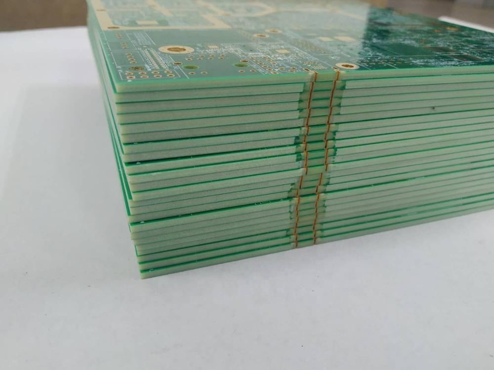
| Layer Count | Up to 64 Layer | 1-68L |
| Max Thickness | 10mm (394mil) | 14mm (551mil) |
| Min Line Width / Space (Inner) | 2.2mil / 2.2mil | 2.0mil / 2.0mil |
| Min Line Width / Space (Outer) | 2.5mil / 2.5mil | 2.2mil / 2.2mil |
| Alignment with Core Board | ±25um | ±20um |
| Inner Layer Alignment | ±5mil | ±4mil |
| Max Copper | 6oz | 30oz |
| Holes Size (Mechanical Drilling) | ≥0.15mm (6mil) | ≥0.1mm (4mil) |
| Holes Size (Laser Drilling) | 0.1mm (4mil) | 0.050mm (2mil) |
| Max Unit Size | 850mm x 570mm | 1000mm x 600mm |
| Max Panel Size | 1250mm x 570mm | 1320mm x 600mm |
| Aspect Ratio (Unit) | 20:1 | 28:1 |
| Aspect Ratio (Panel) | 25:1 | 35:1 |
| Lead-free / Halogen-free Materials | EM827, 370HR, S1000-2, IT180A, EM825, IT158, S1000 / S1155, R1566W, EM285, TU862HF | |
| High-Speed PCB Materials | Megtron6, Megtron4, Megtron7, TU872SLK, FR408HR, N4000-13 Series, MW4000, MW2000, TU933 | |
| High-Frequency PCB Materials | Ro3003, Ro3006, Ro4350B, Ro4360G2, Ro4835, CLTE, Genclad, RF35, FastRise27 | |
| Other Substrates | Polyimide, Tk, LCP, BT, C-ply, Fradflex, Omega, ZBC2000 | |
| Surface Finished | HAL, HAL-LF, ENIG, IMMERSION TIN, OSP, IMMERSION SILVER, GOLD FINGER, Hard Gold/Soft Gold Plating | |
| Special Technology | Blind & buried holes, Via in pad, Semi-plating holes, Counterbore, Step mounting holes, drill Mixed RF PCB, Busbar PCB | |

| Layer Count | Sample Shortest Lead Time | Sample Standard Lead Time | Mass Production Lead Time |
|---|---|---|---|
| 2 layer | 24 h | 3 days | 6-7 days |
| 4 layer | 36 h | 5 days | 8-10 days |
| 6 layer | 48 h | 5 days | 8-12 days |
| 8 layer | 72 h | 5 days | 9-12 days |
| 10 layer | 4 days | 7 days | 14 days |
| 12 layer | 4 days | 7 days | 16 days |
| 14 layer | 5 days | 8 days | 16 days |
| 16 layer | 5 days | 9 days | 18 days |
| 18 layer | 7 days | 10 days | 18 days |
| 20 layer and above | To be negotiated | To be negotiated | To be negotiated |
What types of PCB products do you specialize in?
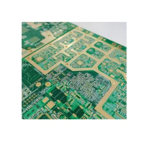
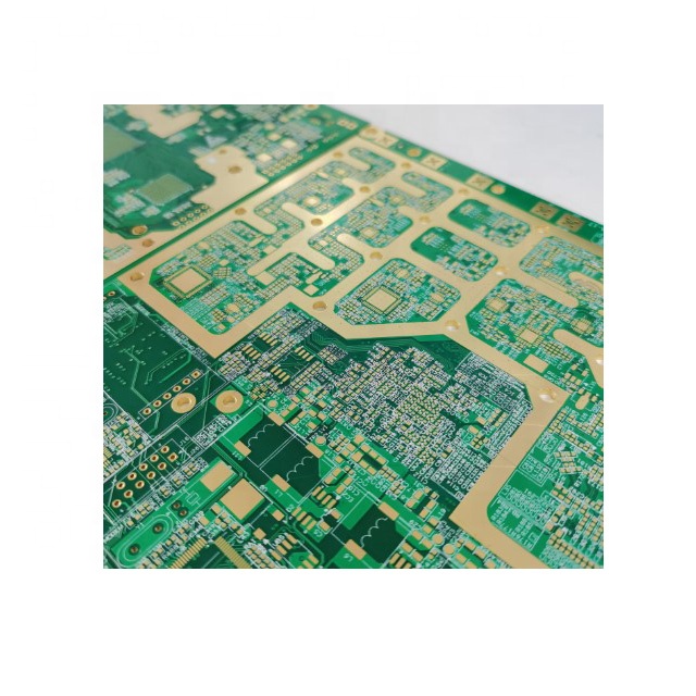
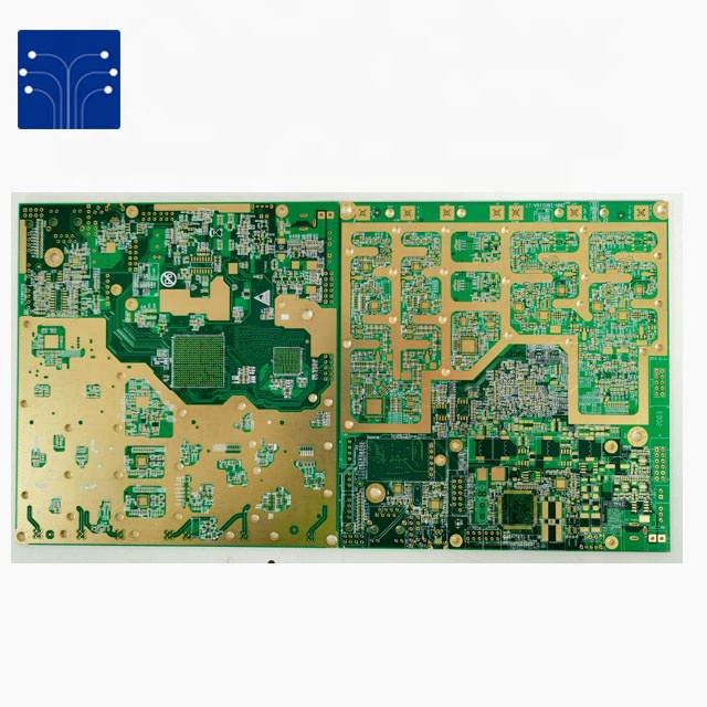
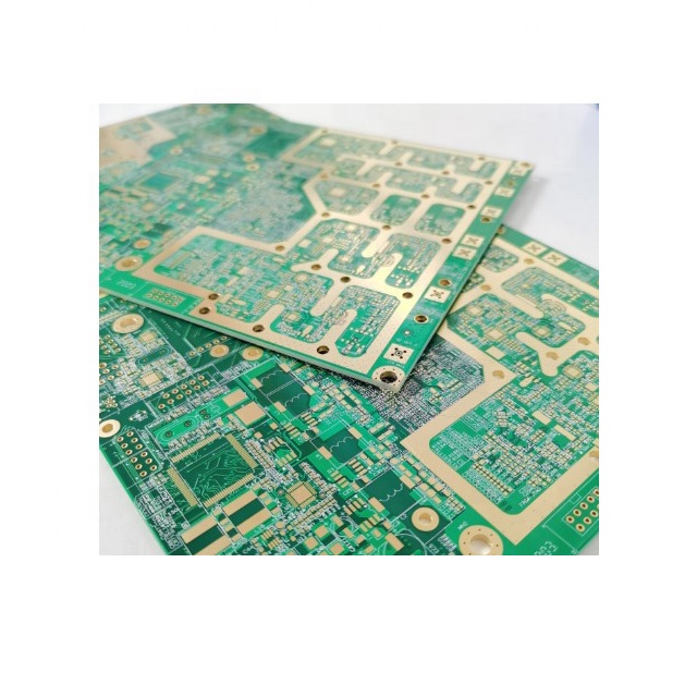
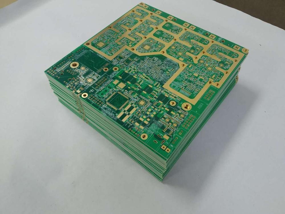
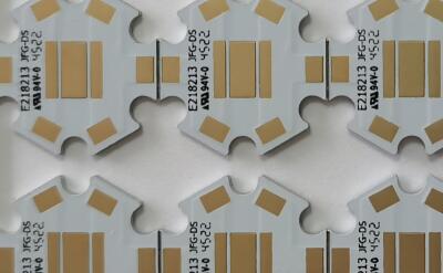
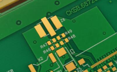
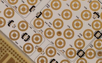
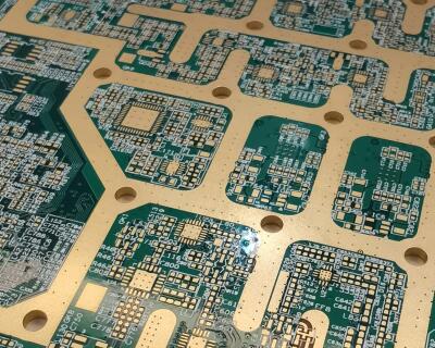
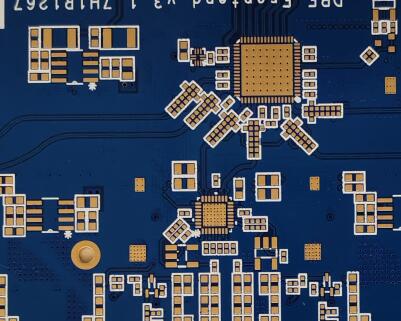
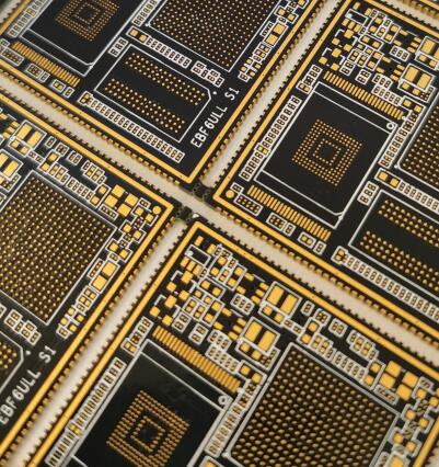
We manufacture a wide range of circuit boards, including high-density multilayer boards (1-68 layers), impedance boards, high-frequency boards, high TG thick copper boards, 5G high-speed boards, buried blind via boards, aluminum-based boards, hybrid dielectric boards, HDI, and rigid-flex boards.
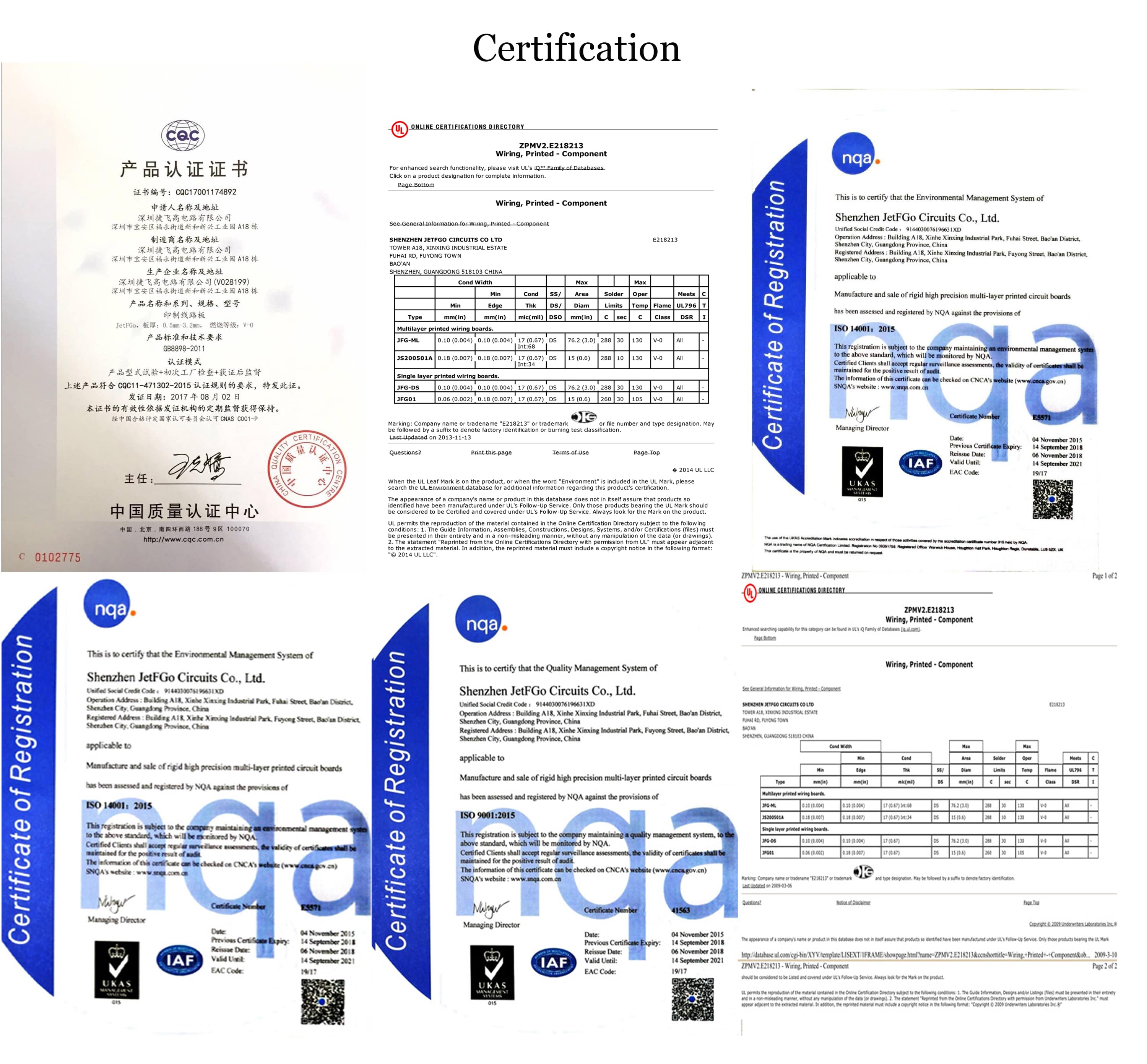
What quality standards and certifications do you support?
Our manufacturing quality conforms strictly to international metrics. We hold credentials including UL, ISO 9001:2015, ISO 14001:2015, CQC, IATF 16949:2016, and National Military Standards, aligning with RoHS and REACH compliance.
What is the fastest turnaround time for prototype samples?
For 2-layer PCBs, we can deliver quick-turn prototypes in as little as 24 hours. 4-layer sample runs take roughly 36 hours, while 6-layer samples can be processed in 48 hours.
What design and Gerber file formats do you accept?
Our engineering department accepts and processes all major CAD/CAM formats, including RS-274-X, RS-274-D, CAD, DXP, Protel 99 SE, PADS, and GC-CAM files.
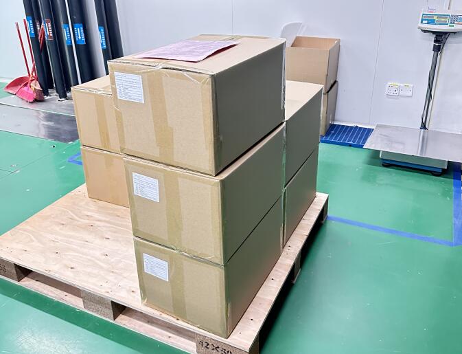
What are your shipment logistics options?
We deliver internationally using air express carriers (UPS, DHL, TNT, CTS, and FedEx), rail freight, and marine cargo. We are also happy to ship via any carrier account designated by our customers.
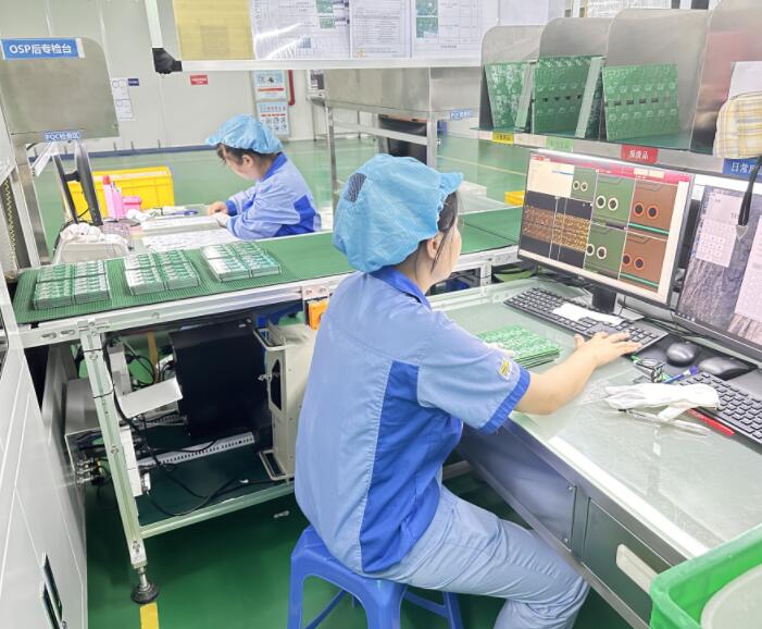
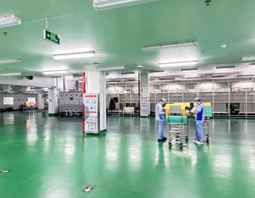
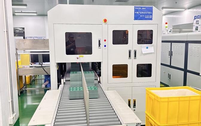
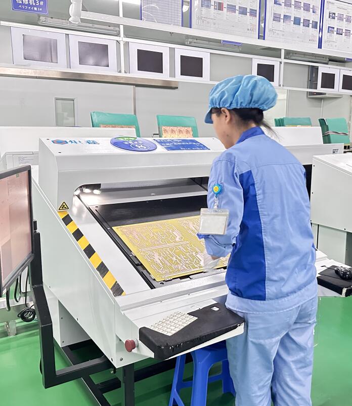
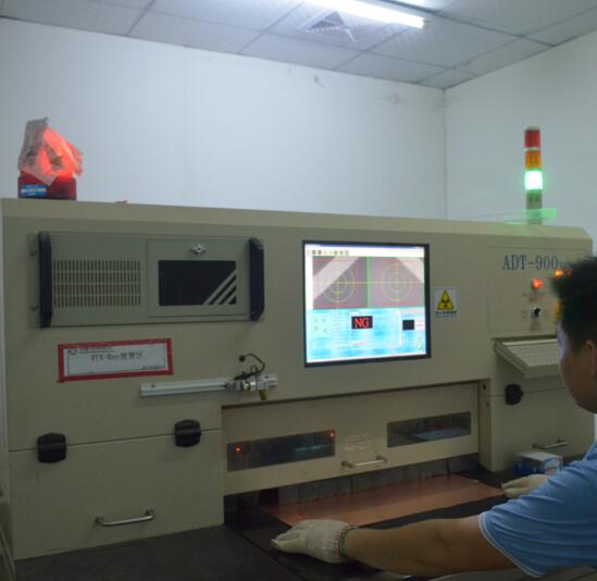
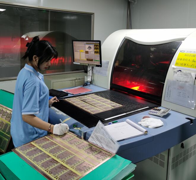
How does your team ensure PCB quality control before shipping?
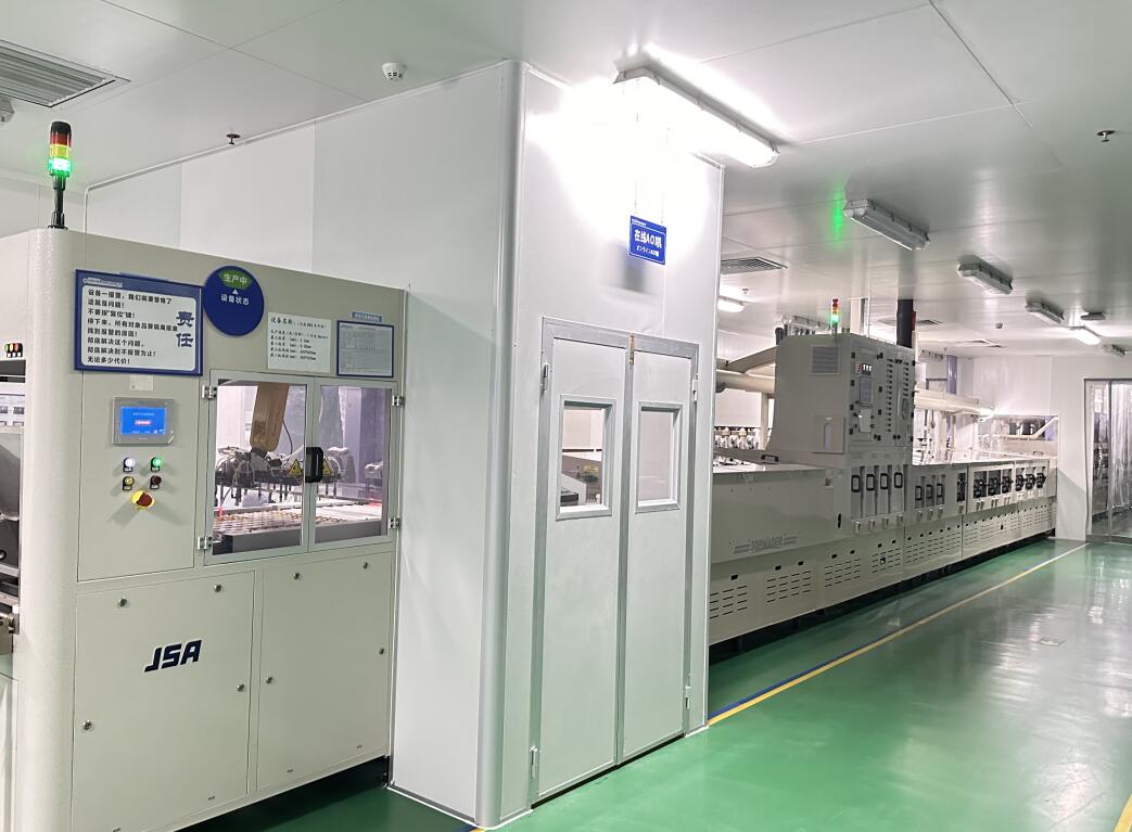
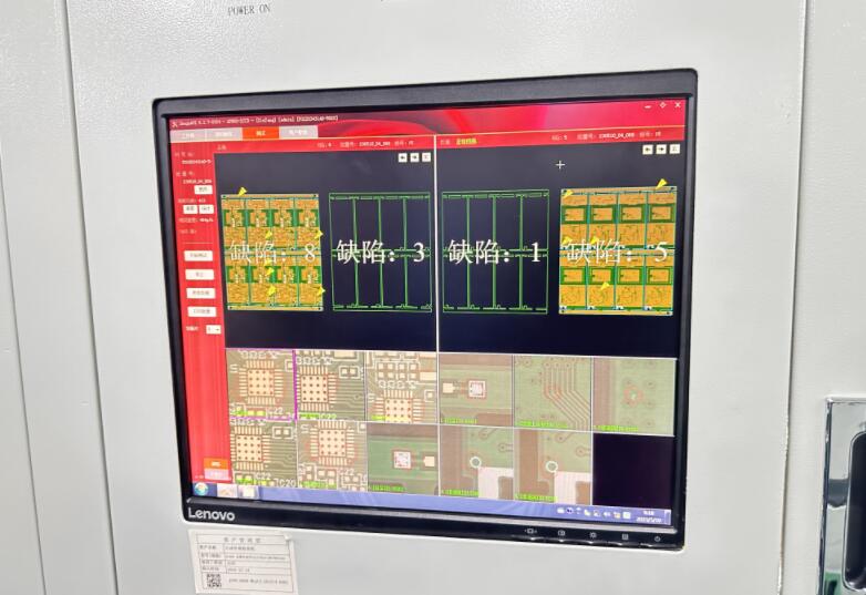
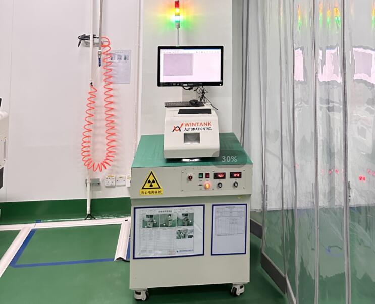
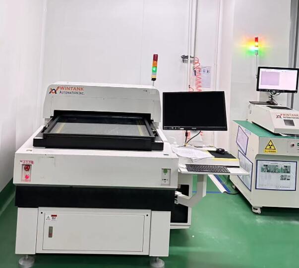
We employ a robust multi-phase QC protocol that integrates AOI, X-Ray inspections, lamination control, thermal shock chambers, and metallographic testing, assuring compliance with customer-specified parameters and IPC guidelines.