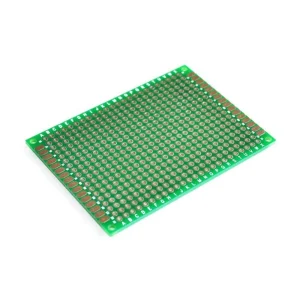
In modern industrial applications, the evolution of high-power electronics requires circuit boards capable of conducting massive electrical currents while maintaining stable thermal thresholds. Thick Copper Circuit Boards (frequently referred to as heavy copper PCBs) feature copper weight distributions ranging from 3 ounces per square foot (oz/ft²) to 20 oz/ft² or more. Standard circuit boards typically rely on 1 oz/ft² (approximately 35μm) of copper, making them insufficient for applications with elevated currents. Thick copper boards supply the cross-sectional trace area necessary to handle high loads without succumbing to thermal stress or circuit degradation.
The core technology behind manufacturing thick copper boards involves a balance of differential etching and specialized plating procedures. Heavy copper plating enables fabricators to increase copper thickness inside plated through-holes (PTH) and via structures, decreasing trace resistance. Consequently, this engineering approach permits a reduction in multi-layer board complexity by integrating high-current power distribution and signal routing onto the same substrate layer. For design engineers, this translates to improved space utilization, simplified system design, and reduced assembly costs.
By leveraging thick copper traces, thermal energy generated by active power semiconductors (such as MOSFETs, IGBTs, and diodes) is distributed directly across the board. The copper acts as a highly efficient heat sink, lowering the operating temperature of surface-mount components and extending the mean time between failures (MTBF) of the entire system.
Globally, the shift toward high-efficiency energy systems has accelerated heavy copper PCB adoption. When manufacturing thick copper designs, designers must consider factors like resin-filling capabilities, laminating tolerances, and dielectric breakdown strengths. Standard FR4 laminates, while suitable for low-power circuits, are often replaced with High-Tg (Glass Transition Temperature) FR4 or metal-clad laminates in heavy copper designs to withstand high thermal loads during solder processing and operations.
As energy generation and electrical vehicle technology scale up, procurement managers and hardware design teams must align their supply chains with the latest heavy copper PCB innovations.
With electric vehicle platforms shifting from 400V to 800V architectures, heavy copper PCBs are replacing traditional busbars. This change optimizes packaging efficiency, reduces vehicular weight, and manages high power loads in on-board chargers (OBC) and power distribution units (PDU).
Artificial Intelligence training engines and high-density enterprise servers require robust power supplies. Heavy copper substrates deliver clean, ripple-free power to advanced processors, preventing voltage drops and structural board failures under variable computation loads.
Utility-scale solar power and offshore wind turbine farms depend on high-efficiency, multi-megawatt power converters. Thick copper PCBs form the core of industrial grid-tie inverters, providing reliable current distribution and resisting environmental wear.
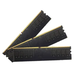
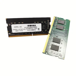
NexaRAM Storage Technology Co., Ltd. is an established DDR5 memory manufacturer specializing in high-performance RAM solutions for B2B OEMs, hyperscale data centers, and critical enterprise computing networks. Established in 2016, our engineers utilize advanced semiconductor substrate manufacturing methodologies to resolve structural thermal design issues. Our core expertise in high-frequency signal integrity and advanced PCB thermal dissipation aligns with thick copper design principles.
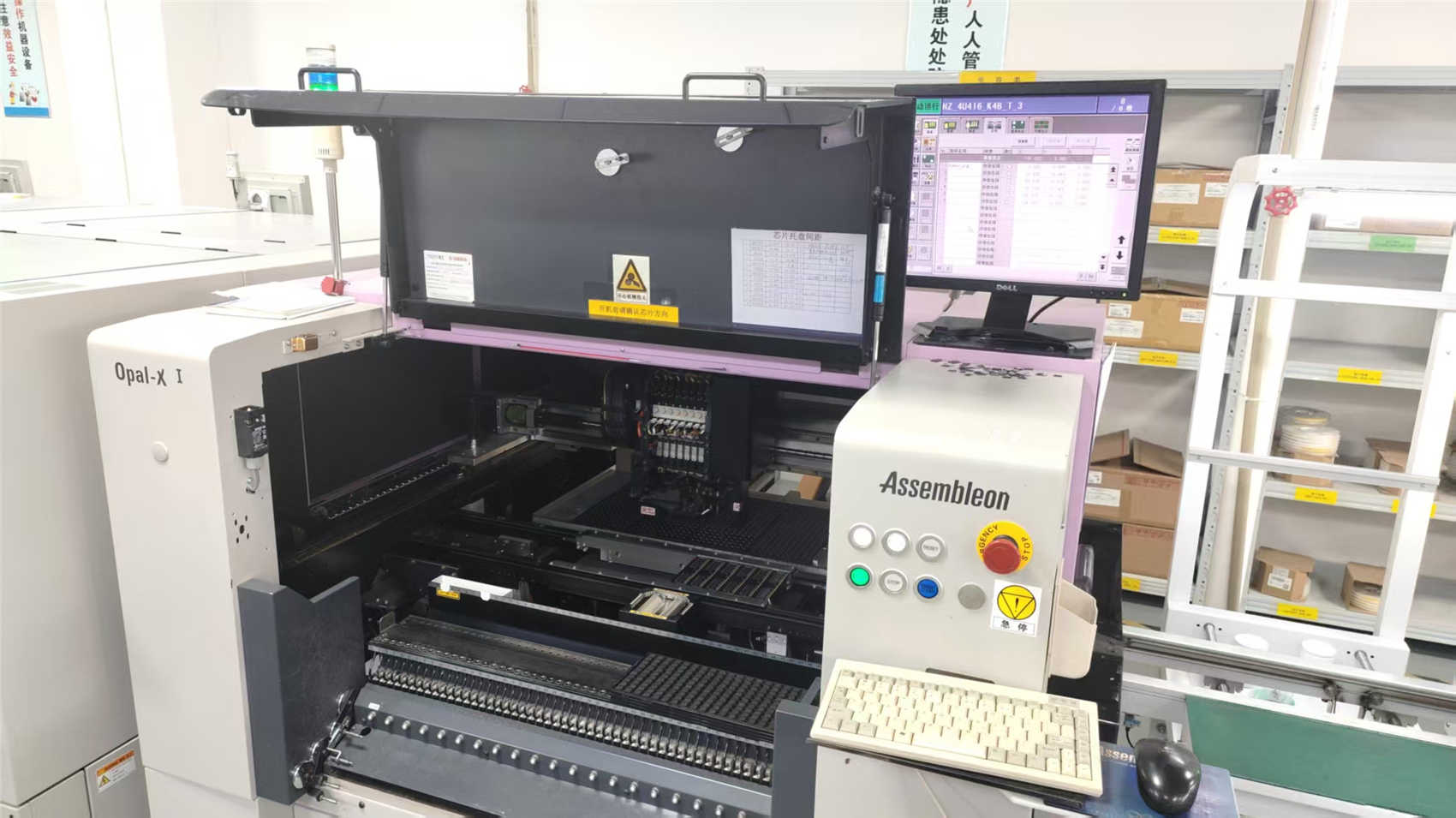
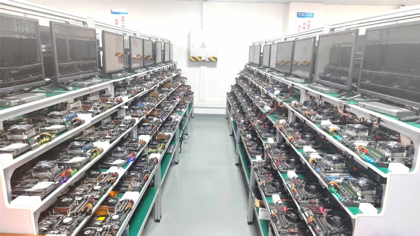
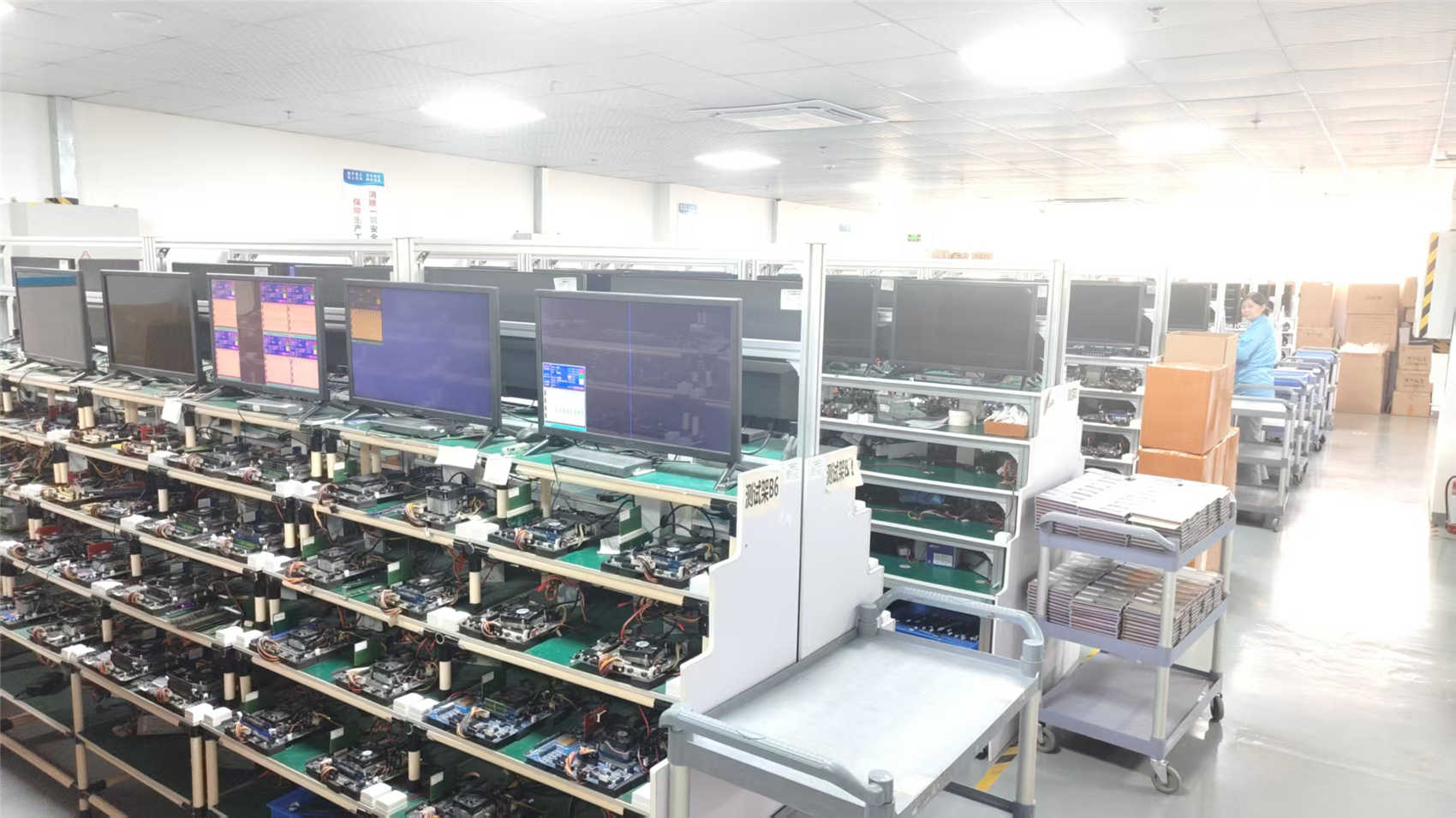
We operate a cleanroom manufacturing facility spanning approximately 320㎡. Equipped with advanced automated placement and high-volume optical verification lines, NexaRAM secures an annual export volume of USD 12 million. Supported by 6 years of direct export operations and 12 years of industry experience in DRAM packaging and PCB engineering, our team is qualified to assist with complex hardware designs.
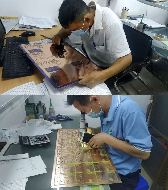
Quality control is maintained using automated optical inspection (AOI) systems alongside temperature-cycled burn-in testing. These steps are overseen by our team of 35 QC inspectors. Backed by 850 strategic supply chain partners, we ensure uninterrupted procurement of raw copper foil, high-Tg FR4 laminates, and active components. This supply chain stability protects against material shortages and price fluctuations.
Step inside our cleanroom fabrication facilities. We apply real-time tracking, quality control inspections, and diagnostic instruments to ensure high yield rates on thick copper substrates and memory modules.


The manufacturing process for heavy copper circuit boards requires strict thermal control and chemical precision. China's shift to Factory 4.0 paradigms integrates automation, big data analysis, and eco-friendly manufacturing technologies to secure production. Advanced chemical plating baths use automated monitoring systems to ensure uniform copper deposition on thick traces. This minimizes trace thinning at corners, which can cause hot spots during operation.
Furthermore, China's manufacturing ecosystem features vertical integration, placing raw copper laminates, glass fiber, epoxy resin suppliers, and advanced packaging plants within the same region. This minimizes lead times, allowing Chinese suppliers to scale production from prototype runs to high-volume manufacturing within days. This geographic concentration reduces geopolitical and transport risks, providing global partners with pricing stability.
NexaRAM operates in alignment with these standards. Our engineering team of 180 researchers released 120 product variants last year. This demonstrates our ability to convert design requirements into production-ready solutions. By using smart logistics systems, real-time tracking, and automated material replenishment (MRP), we coordinate with partners across North America, Europe, Southeast Asia, and the Middle East to deliver components on time.
In hot desert environments like the Middle East (e.g., NEOM project zones), outdoor combiner boxes face extreme ambient heat and high operational currents. Using 6 oz thick copper boards allows system builders to replace discrete copper wires with single, consolidated PCB backplanes. This design eliminates manual wiring errors, withstands ambient heat, and resists vibrations caused by sandstorms.
European Tier-1 automotive integrators must meet strict safety and packaging standards (such as ISO 262262 and IPC Class 3). Custom multi-layer heavy copper boards solve space limitations inside vehicle drivetrains. By embedding logic circuits next to the high-power traction stage, engineers save weight and lower assembly costs compared to separate busbar arrangements.
North American utility substations face extreme temperature drops during winter. Standard power supplies can suffer structural trace fractures due to CTE (Coefficient of Thermal Expansion) mismatch between copper and laminate materials. Heavy copper PCBs, with their robust structural builds, endure rapid temperature changes and prevent cracking, ensuring consistent performance in remote power stations.
A thick copper board (or heavy copper PCB) typically refers to a circuit board that has copper conductor layers thicker than 3 oz/ft² (105μm). Standard PCBs rely on 1 oz/ft² copper. These heavy copper boards are designed to handle high current demands and thermal loads without trace failures.
Current-carrying capacity is proportional to the cross-sectional area of the copper trace. For a given trace width, increasing copper thickness (e.g., from 1 oz to 6 oz) reduces electrical resistance, which lowers heat generation under high current loads.
Thick copper traces act as integrated heat sinks. They distribute heat away from components like power transistors across the board's surface, lowering operational temperatures and reducing the need for heavy external heat sinks.
Heavy copper PCBs generally feature copper weights between 3 oz/ft² and 19 oz/ft². Extreme copper PCBs refer to designs with copper weights from 20 oz/ft² up to 200 oz/ft². These are used in heavy-duty utility and industrial installations.
Key challenges include control of chemical etching to prevent undercut, achieving proper resin fill between high traces during lamination, and managing thermal contraction differences between copper and substrate material to prevent warping.
NexaRAM maintains quality by combining Automated Optical Inspection (AOI) with burn-in testing. We select high-Tg base laminates and use automated chemical monitoring during copper plating to ensure stable board construction.
For heavy copper boards, we recommend High-Tg FR4 laminates (Tg170 or Tg180) to handle thermal expansion. In specialized systems, metal-clad or ceramic-filled substrates are used to further improve heat dissipation.
Thick copper requires wider trace spacing. For example, a 3 oz copper trace typically requires a minimum spacing of 10-12 mils to prevent chemical bridging, and wider traces are needed to account for undercut during etching.
Heavy copper boards should meet the IPC-A-600 Class 2 or Class 3 standards, which define plating thickness and structural integrity. Solderability and thermal shock testing are also conducted to verify performance.
Factory 4.0 setups integrate real-time tracking with automated chemical controls. This monitors copper plating parameters continuously, keeping plating thickness within tight specifications and minimizing human assembly errors.