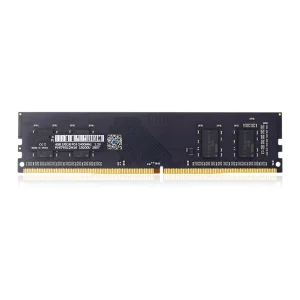
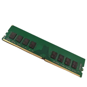
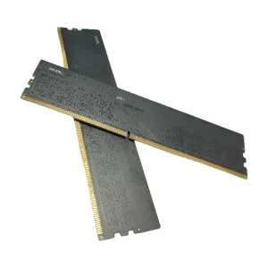
Premium precision memory components and SMT tooling solutions deployed across Melbourne's high-tech manufacturing sector.
Melbourne has consolidated its position as Australia's leading hub for advanced manufacturing, high-value electronics engineering, and prototyping. From industrial corridors in Dandenong, Clayton, and Port Melbourne to the innovative medical technology precincts, the demand for High-Density Interconnect (HDI) Printed Circuit Board Assemblies (PCBAs) is growing rapidly. Modern electronics, such as aerospace telemetry, advanced automotive sensory arrays, IoT sensors, and high-frequency communication motherboards, require components with sub-millimeter pitches.
At the core of the SMT assembly line lies the solder paste printing process, which accounts for over 60% of all SMT defects. To achieve high yield rates and reliability, electronics manufacturing services (EMS) providers in Melbourne rely on high-precision laser-cut stencils. As a specialized stencils factory and exporter, we design products tailored to meet the challenges of the Victorian market. Our stencils ensure accurate volume deposit control, clean paste release, and minimal bridging for complex footprints, including 01005 passives, micro-BGAs, and fine-pitch QFNs.
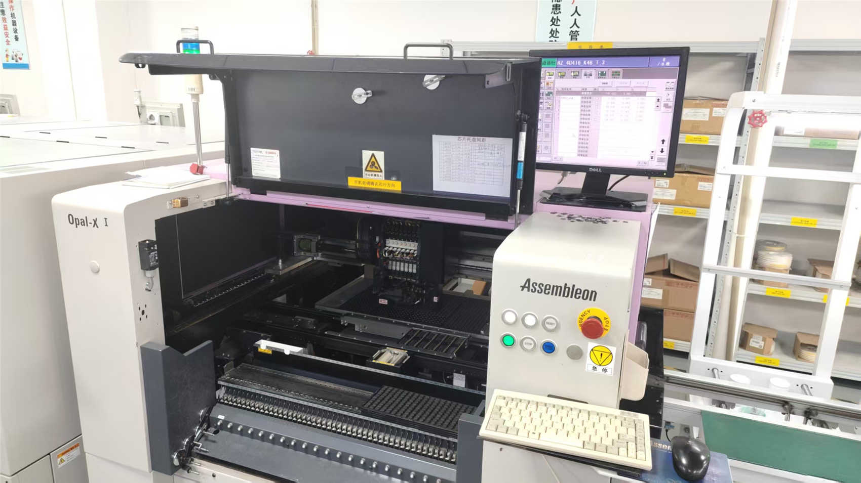
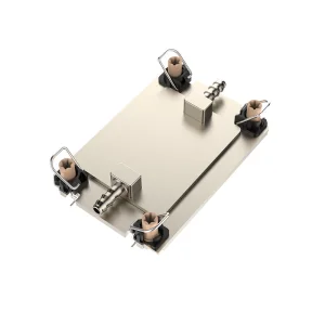
Figure 1: NexaRAM's ISO 9001 certified production facility featuring advanced SMT layout testing systems.
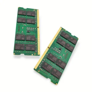
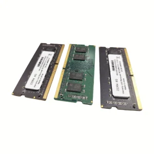
Bridging advanced DRAM semiconductor module manufacturing with custom tooling stencils for international markets.
Operating as a division of NexaRAM Storage Technology Co., Ltd., we utilize deep expertise in high-frequency semiconductor layout, DDR5 signal integrity, and high-performance server thermal configurations. Since 2016, our manufacturing centers have delivered advanced memory solutions and custom stencils globally. Our facilities span over 320㎡ of cleanroom-grade space optimized for high-precision tooling fabrication, automated optical inspection (AOI), and comprehensive burn-in testing.
Our background in DRAM and high-speed memory module fabrication gives us a unique advantage in stencil engineering. Designing stencils for DDR4/DDR5 packages requires a deep understanding of micron-level pad spacing, aspect ratios, and thermal sink constraints. Our engineers apply these principles to every custom laser stencil exported to Melbourne, ensuring each aperture configuration minimizes solder voiding and achieves high printing repeatability.
The performance of a laser-cut stencil depends on sheet thickness selection, aperture shape design, and wall roughness control. Our stencils are cut from premium-grade stainless steel using high-precision fiber laser systems. These systems maintain dimensional tolerances within ±5μm, enabling clean cut geometries and precise aperture wall taper angles (typically 1.5° to 2° to optimize solder paste release).
To prevent paste sticking to the aperture walls, we apply IPC-7525 standard equations for all layout designs:
Area Ratio = Area of Aperture Opening / Area of Aperture Walls (Must be > 0.66 for standard solder paste printing)
Aspect Ratio = Width of Aperture / Thickness of Stencil Foil (Must be > 1.5 to maintain mechanical integrity)
Our engineers use CAD tools to verify these ratios across your design before production. If an aperture fails to meet these thresholds, we recommend localized step-down stencils or nano-coatings to ensure reliable printing.
| Parameters | Standard Laser Stencil | Step-Down / Step-Up Stencils | Electroformed Nickel Stencils |
|---|---|---|---|
| Foil Material | SUS304 / FG (Fine Grain) Stainless Steel | SUS304 / Special Alloy Foils | 100% Electrodeposited Nickel |
| Thickness Range | 0.08 mm - 0.25 mm (±3% Tolerance) | 0.06 mm - 0.30 mm (Variable Steps) | 0.03 mm - 0.15 mm (±1.5% Tolerance) |
| Minimum Aperture Width | 80 μm (0.08mm) | 70 μm (0.07mm) | 40 μm (0.04mm) |
| Aperture Wall Roughness | < 1.5 μm (Ra) | < 1.2 μm (Ra) | < 0.2 μm (Ra) (Mirror Surface) |
| Key Applications | Standard FR4, QFN, 0402 component arrays | Mixed technology PCBs, RF shields, connectors | Ultra-fine pitch BGAs, Wafer bumping, 01005s |
For high-density designs, we offer hydrophobic and oleophobic nano-coatings. These coatings are applied as an ultra-thin polymer layer on the bottom surface and inside the walls of the stencil. This treatment reduces solder paste sticking, decreases under-stencil cleaning cycles, and limits bridging defects. For Melbourne EMS factories using high-speed automatic printers, our nano-coated stencils can improve paste transfer efficiency by up to 25% on micro-BGA pads.
A look inside our QA facilities, where high-speed AOI machines and custom testing fixtures verify compliance with IPC standards.
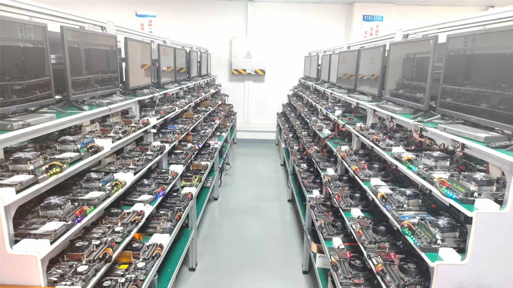
Figure 2: Automated inspection laboratory verifying aperture tolerances.

Figure 3: Optical inspection systems measuring stencil aperture walls.
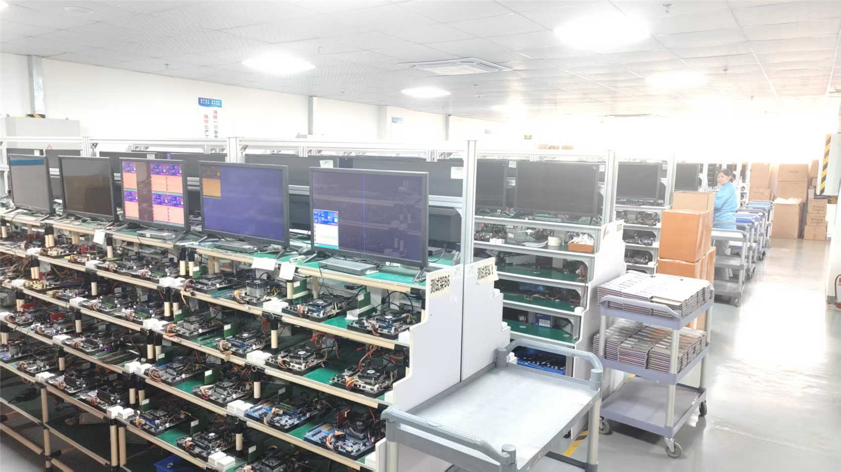
Figure 4: Automated calibration jigs validating custom memory PCB dimensions.
Quality control is integrated throughout our manufacturing process. We maintain a team of 35 dedicated QC inspectors who oversee operations from steel foil arrival to final export shipping. Stencils undergo 100% Automated Optical Inspection (AOI) to verify that all apertures are cut according to the customer's Gerber specifications. We verify coordinates, check for micro-burrs, and ensure alignment fiducials are clean. This level of quality management minimizes the risk of stencil defects arriving at your Melbourne production line.

Figure 5: High-speed Pick-and-Place systems running memory module production lines.
We work to support local production cycles in Melbourne. Understanding that SMT lines operate on strict schedules, we optimize our design, cutting, and export processes to minimize lead times. Orders are processed, checked, and fabricated within 24 to 48 hours, followed by express air shipping to Melbourne Tullamarine Airport for fast delivery to your factory floor.
Our stencils and packaging materials comply with Australian biosecurity standards. Frame-mounted stencils use export-grade aluminum profiles and compliant packaging, eliminating customs clearance delays. Every product is supplied with chemical compliance and RoHS testing reports to meet Victorian environmental guidelines.
We support local technical engineering teams with comprehensive data processing options. We accept Gerber, ODB++, and DXF formats. Our design engineers can apply global standard modifications (such as homeplate, bow-tie, and rounded corner adjustments) to suit specific paste chemistry and component requirements.
As electronics design transitions toward IoT integration, flexible hybrid electronics (FHE), and advanced automotive driver systems (ADAS), stencil manufacturing must continue to evolve. NexaRAM keeps pace with these industry changes by investing in modern manufacturing tools and processes:

Figure 6: Automated fiber laser calibration setup.

Figure 7: Raw material warehouse inventory management.

Figure 8: Compliance laboratory checking physical stencil parameters.
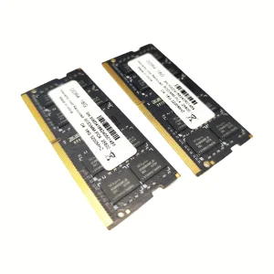
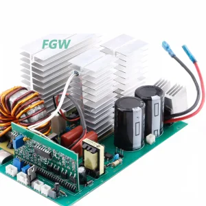
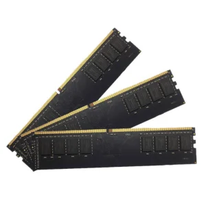
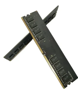
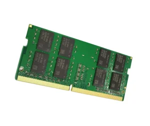
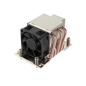
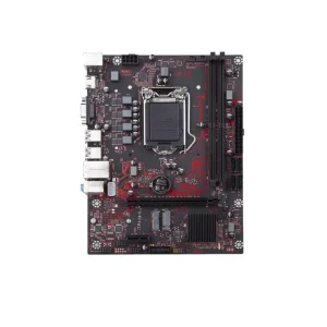
A selection of industrial system components, PCB assemblies, and cooling solutions engineered for reliability in challenging operating conditions.
Additional products from our technical catalog, including radiators, cooling units, and processor platforms.
Developing effective PCB stencils requires a combination of high-precision cutting technology and experienced software engineering. Our team of 180 engineers works to refine aperture design methodologies. We optimize apertures for difficult components like edge connectors, thermal ground pads, and fine-pitch arrays. In the past year, we have introduced 120 new product variations and updates, including multi-level step stencils and advanced nano-coating applications.
We work closely with 850 strategic supply chain partners to source high-grade metal foils, including poly-crystalline steel, fine-grain materials, and electroformed nickel. This allows us to supply stencils that maintain dimensional stability under varying temperature and humidity conditions in your factory.
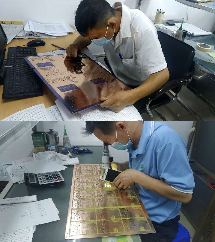
Figure 9: R&D engineering team analyzing PCBA Gerber layouts before laser processing.
Answers to common technical, logistics, and compliance questions regarding our stencils and services in Melbourne.
Our standard manufacturing turnaround time is 24 to 48 hours from design approval. We utilize express air freight to Melbourne, resulting in a typical door-to-door delivery time of 3 to 5 business days. We provide tracking information to help you manage your production scheduling.
We analyze the component footprints on your PCB. If you have a mix of large power components requiring high solder volume and fine-pitch BGAs requiring minimal deposit, we recommend step-up or step-down stencils. This allows us to achieve different foil thicknesses on a single stencil sheet.
Yes, we manufacture both framed and frameless stencils. Our frameless stencils are compatible with standard quick-change frame systems, including ZelFlex, LPKF, and VectorGuard. Frameless options help reduce shipping costs and require less storage space in your facility.
Every stencil undergoes 100% Automated Optical Inspection (AOI) to check aperture geometry, dimensions, and positioning. We verify that all parameters match your submitted Gerber files prior to packaging and shipping.
Get in touch with our design engineers for a technical review of your Gerber layouts, custom aperture modifications, and a detailed quotation for high-precision laser-cut stencils.