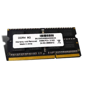
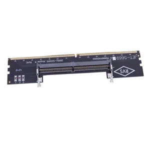
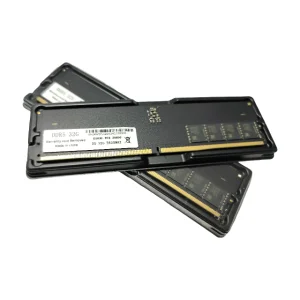
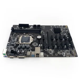
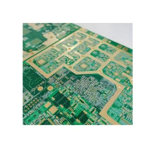
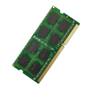
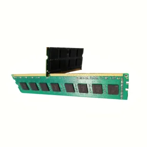
Direct access to our engineered semiconductor layouts, motherboard chipsets, and high-frequency memory hardware optimized for rapid surface mount assembly.
In the rapidly scaling electronics manufacturing services (EMS) landscape, the precision of solder paste deposition represents the single most critical factor determining overall assembly yield. Over 65% of all SMT defects—such as bridging, insufficient solder, and voiding—trace their origins directly to the stencil printing process. As component packages shrink from 0603 and 0402 down to ultra-fine-pitch BGAs, QFNs, and passive 01005 chips, the tolerances allowed for stencil manufacturing have narrowed to micro-levels.
Laser-cut stencils represent the pinnacle of stencil printing technology. Utilizing ultra-precise German-engineered fiber laser systems, apertures are cut with a positional accuracy of ±2μm. The taper of the aperture walls is controlled to facilitate optimal solder paste release. By establishing highly polished aperture walls, paste transfer efficiency is maximized. This is particularly crucial for modern multi-layered boards hosting high-speed storage modules, high-frequency RF components, and complex logic motherboards.
Indonesia is accelerating its industrial transformation under the "Making Indonesia 4.0" initiative, placing a strong emphasis on localized electronics manufacturing, automotive assemblies, and internet-of-things (IoT) devices.
The country’s electronics manufacturing ecosystem is concentrated in three main zones: the Bekasi-Cikarang-Karawang Industrial Corridor in West Java, the Batam Free Trade Zone close to Singapore, and metropolitan Jakarta. High-volume consumer electronics, smart energy meters, telecom equipment, and automotive control modules are assembled in these zones. Each of these applications requires custom SMT stencils that can handle different paste volume requirements.
In coastal and high-humidity areas like Batam or Jakarta, SMT processes face distinct climate-related challenges. Relative humidity levels above 60% can rapidly degrade solder paste viscosity, causing slumping and subsequent bridging on fine-pitch components. This makes the engineering of the laser stencil even more critical. Our stencils feature advanced hydrophobic nano-coatings and micro-machined step-up/step-down geometries to mitigate these environmental challenges, ensuring stable solder print deposits under varying cleanroom climates.

Sourcing precision tools like laser stencils, high-frequency PCBs, and advanced memory modules from China offers a competitive edge in speed, cost, and design flexibility. The manufacturing ecosystem integrates material suppliers, laser machinists, plating specialists, and international shipping lanes into a single, cohesive workflow.
Our factory utilizes premium fine-grain FG360 stainless steel foils, known for superior yield strength and clean edge properties. By combining these materials with automated optical inspection systems and computerized laser paths, we cut down SMT stencil production times to under 24 hours from CAD approval. Direct air shipping networks connecting Shenzhen and Hong Kong to Soekarno-Hatta (CGK) and Hang Nadim (BTH) ensure that customized tooling arrives at your assembly line within 3 to 5 business days.
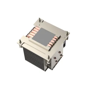
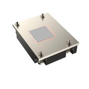
A complete selection of advanced hardware to optimize processing architectures, high-frequency communication, and thermal management in heavy industrial environments.
For manufacturing engineers looking to maximize first-pass yield, designing stencils involves balancing geometry, material chemistry, and surface finishes.
An essential design rule for SMT printing is the Area Ratio (AR). The Area Ratio is defined as the area of the aperture opening divided by the surface area of the aperture walls. To achieve clean solder paste release, industry guidelines state that the Area Ratio should be greater than 0.66:
Area Ratio (AR) = [ W × L ] / [ 2 × T × (W + L) ] > 0.66
Where W represents the aperture width, L represents the aperture length, and T represents the thickness of the stainless steel stencil foil. When printing paste for micro-BGAs or 01005 passives, standard square or circular apertures may fall below this threshold. In these scenarios, stencil manufacturing must leverage electro-polishing or active nano-coating treatments to reduce the coefficient of friction on the aperture walls.
| Stencil Technology Type | Typical Aperture Wall Roughness (Ra) | Minimum Aperture Width (Pitch) | Recommended SMT Paste Type | Best Application Match |
|---|---|---|---|---|
| Standard Laser Cut Stencil | 0.8 μm - 1.2 μm | 0.4 mm | Type 3, Type 4 | General SMT Assembly, Consumer PCBs |
| Electro-Polished Laser Stencil | 0.3 μm - 0.5 μm | 0.3 mm | Type 4, Type 5 | Fine-Pitch QFN, High-Density Motherboards |
| Nano-Coated Laser Stencil | < 0.2 μm (Ultra Smooth) | 0.25 mm | Type 5, Type 6 | 01005 Passives, High-Speed DDR5 Layouts |
| Step-Up / Step-Down Stencil | Varies based on section | Mixed pitch variable | Mixed paste types | Automotive & Power Electronics with Shield Cans |
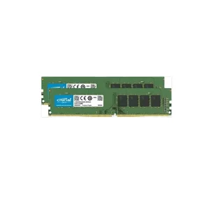
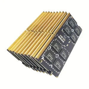
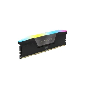
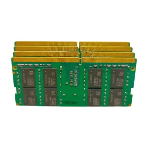
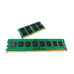
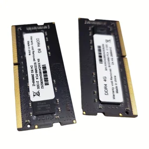
NexaRAM Storage Technology Co., Ltd. is a professional DDR5 memory manufacturer specializing in high-performance RAM solutions for global OEMs, data centers, and enterprise computing applications. Established in 2016, the company has rapidly developed into a reliable supplier in the advanced DRAM industry.
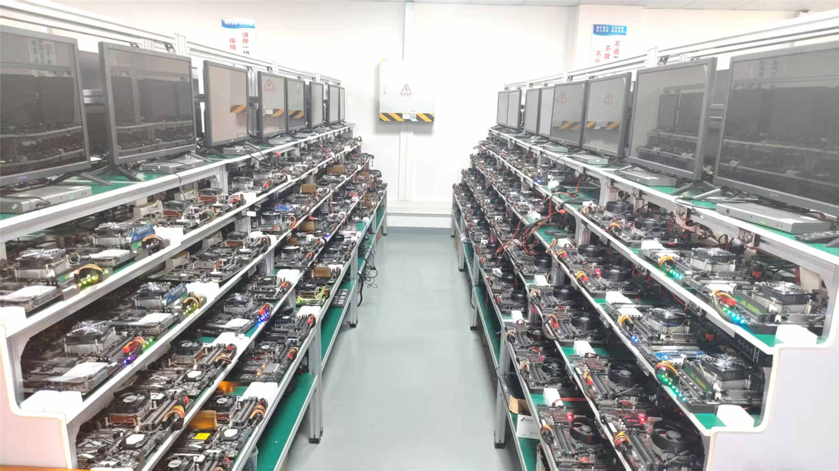
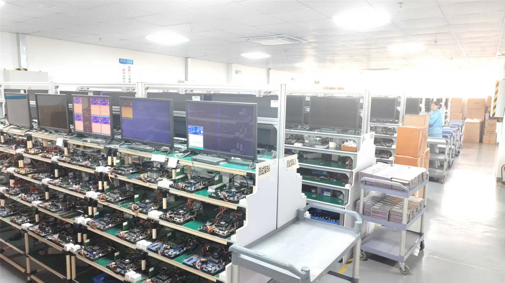
The company operates a modern production facility with a total building area of approximately 320㎡, equipped with advanced manufacturing and testing equipment to ensure stable and efficient production capacity. NexaRAM has an annual export revenue of approximately USD 12 million, with 6 years of export experience and 12 years of industry experience in memory and semiconductor-related fields.
Quality is strictly controlled through a combination of automated optical inspection (AOI) and burn-in reliability testing, supported by a professional QC team of 35 inspectors. The company follows international trade compliance standards and operates under a strong global trading background, serving markets across North America, Europe, Southeast Asia, and the Middle East.
NexaRAM maintains a highly developed supply chain ecosystem with over 850 strategic supply chain partners, enabling stable sourcing of high-grade semiconductor materials and components. Its primary customer base includes OEM manufacturers, system integrators, server solution providers, and gaming PC brands.
The company demonstrates strong R&D capabilities, offering custom DDR5 module design, PCB layout optimization, frequency tuning, and thermal solution development. Flexible customization options include frequency, latency, capacity, heat spreader design, and branding services.
In the past year, NexaRAM launched 120 new product variants, supported by a dedicated R&D team of 180 engineers, continuously driving innovation in high-speed memory solutions for next-generation computing systems.
A clean view of our design, quality control, logistics footprint, and industrial capacity supporting partners in Indonesia and worldwide.
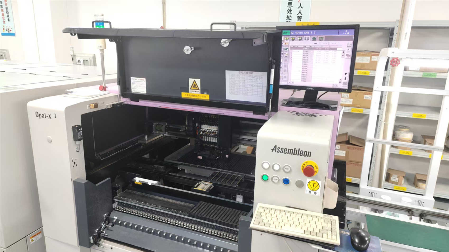
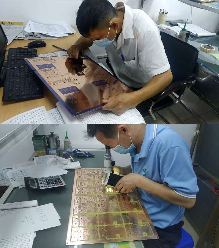
Providing transparent proof of our operations. Real scenes from our ISO-compliant testing laboratory, cleanrooms, and high-precision inspection lines.


Explore our full catalog of high-frequency substrate layers, thermal mitigation assemblies, and memory architectures ready for delivery to Indonesian industrial zones.
Understanding technological developments helps modern buyers optimize their material sourcing strategies and design decisions.
1. The Rise of Multi-Level Step Stencils: Modern system-on-module designs place high-density computing components directly adjacent to larger connecters or shield brackets. Standard single-thickness foils are no longer sufficient. Localized step-up and step-down stencils are becoming the standard, allowing operators to deposit different solder volumes on a single board layout.
2. Hydrophobic Nano-Coatings: Advanced hydrophobic/fluxphobic coatings are applied to the underside and aperture walls of laser-cut stencils. This reduces cleanroom maintenance cycles, lowers the risk of solder bridging, and improves paste release metrics on dense component designs.
3. Clean Green Manufacturing: Environmental regulations are driving the adoptation of lead-free solder profiles and eco-friendly stencil cleaning solvents in Indonesian assembly hubs. We optimize our aperture geometries to support the higher surface tensions typical of lead-free and halogen-free paste chemistries.
From the moment the Gerber data is verified and CAD designs are approved, our production is completed within 24 hours. Transit to major Indonesian hubs, including the Jakarta metropolitan area (Bekasi, Cikarang) and Batam, takes 3 to 5 business days using air freight channels.
To counter potential solder paste slumping and bridging caused by high relative humidity, we recommend stencils treated with advanced nano-coatings. These coatings repel flux residues and keep the stencil cleaner during print cycles. We also fine-tune aperture reduction ratios in CAD layouts to compensate for humidity-related paste flow behavior.
We use high-grade, fine-grain FG360 stainless steel foils. This material provides excellent tension stability and clean aperture edges, outperforming standard steel foils under continuous printing cycles.
Yes. Through our manufacturing partners and integrated supply chains, we offer comprehensive PCB design layout optimization, frequency tuning, thermal simulations, and customized step stencils to support high-density component arrays.
Our quality control processes combine Automated Optical Inspection (AOI) with physical verification. We inspect laser stencil aperture sizes and wall smoothness to ensure they match customer CAD designs before shipment.