Reliable components designed for next-generation telecommunications, server infrastructure, and industrial optical-to-electrical interfaces.
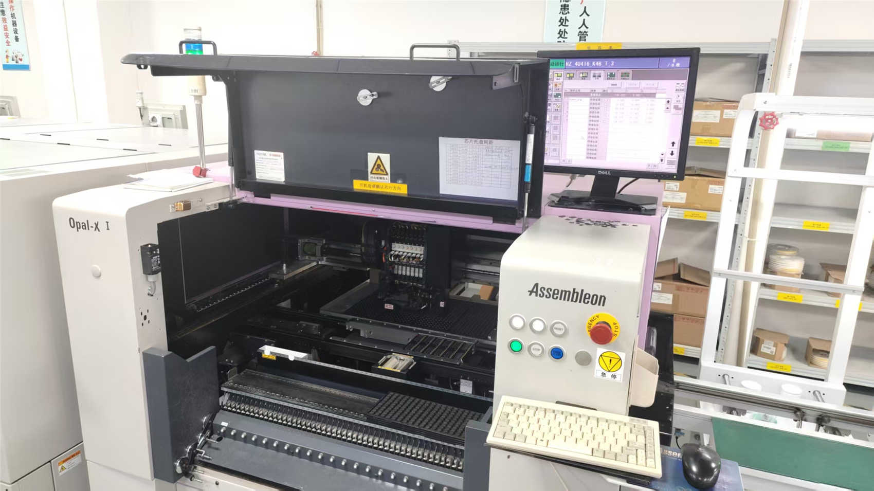
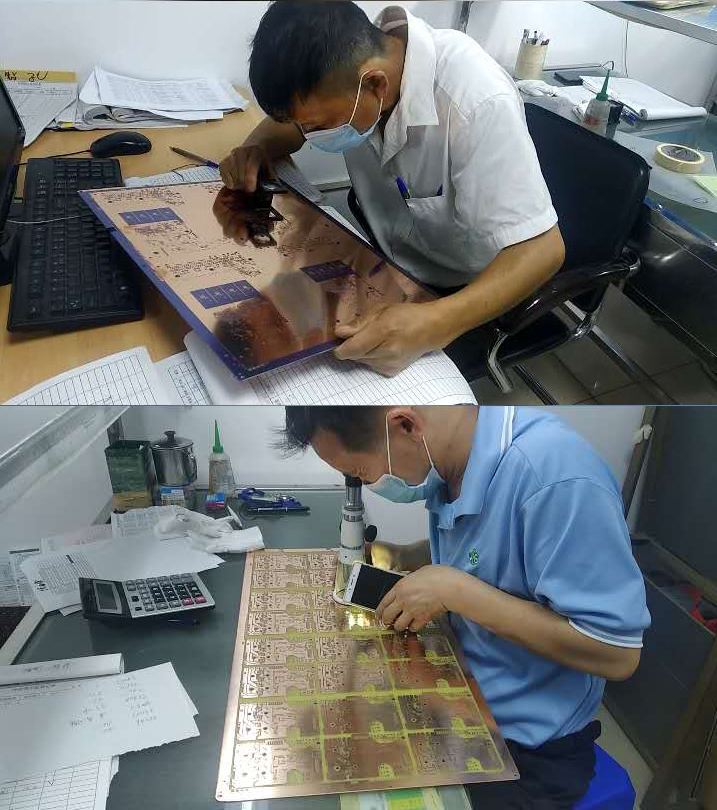
Inside our high-precision production environment, where optical and electronic components undergo rigorous quality assurance.
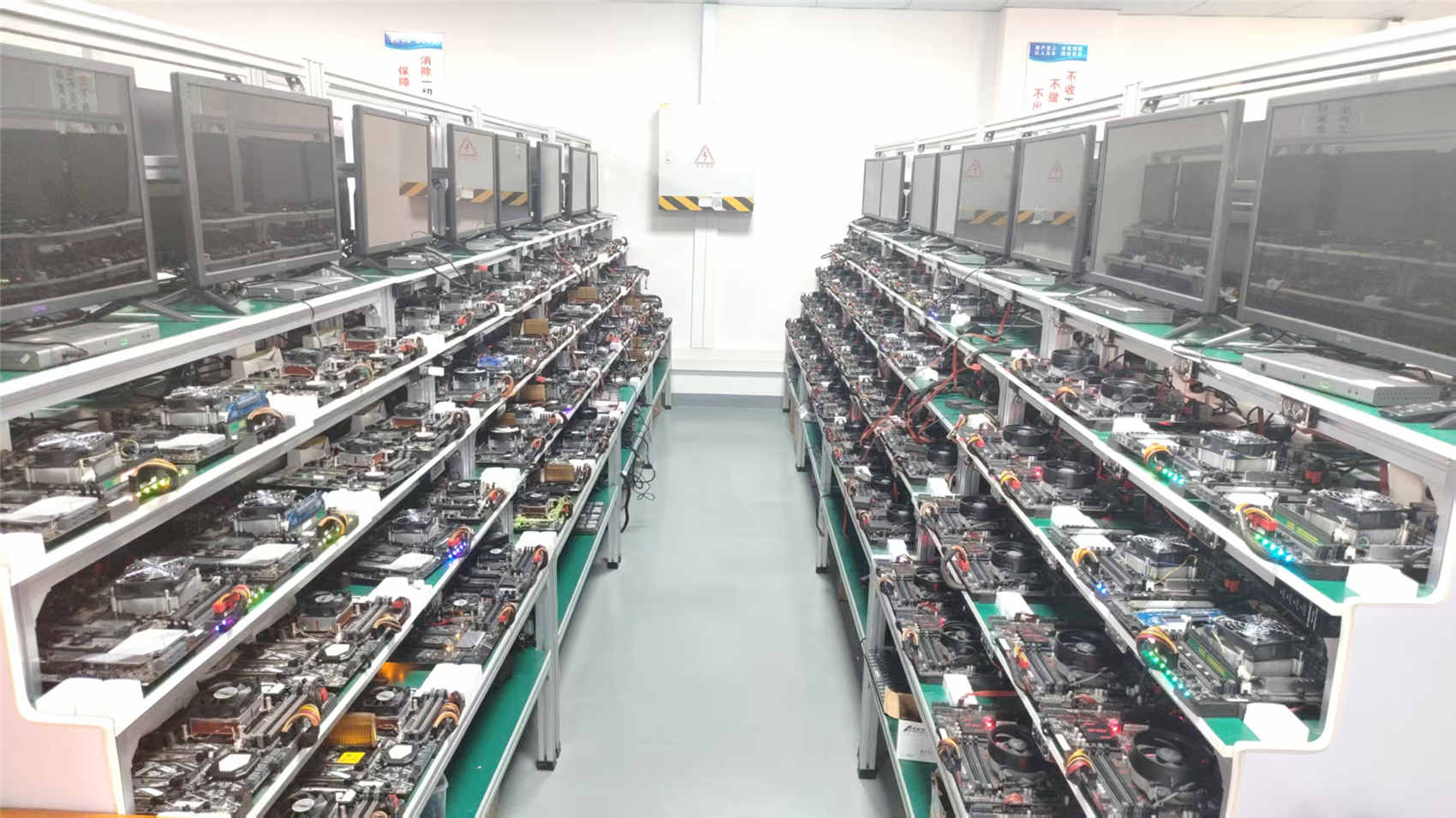

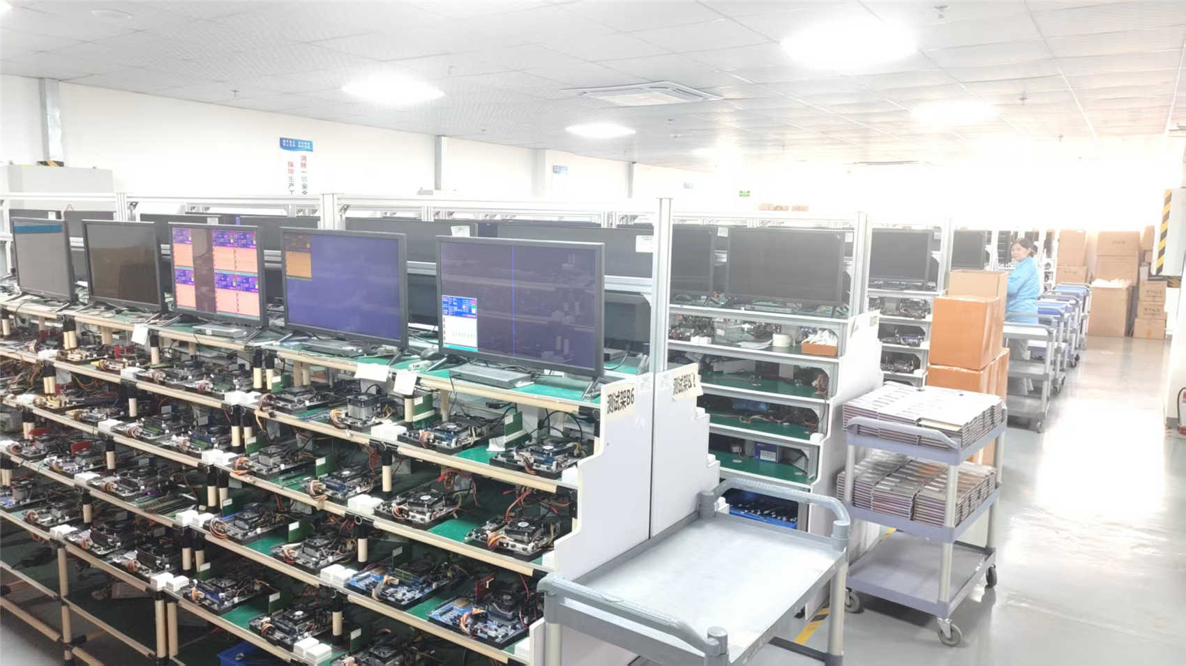


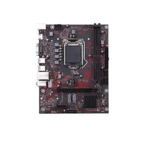
Industrial server modules, computer motherboard setups, custom high-output heat sinks, and renewable energy conversion components.
Our specialized R&D engineering team works directly with client system designers to customize high-frequency substrate architectures. By deploying advanced PCB layout techniques, signal routing simulations, and choosing specific low-dissipation factors (Df) and dielectric constant (Dk) materials, we ensure that the PCB assembly remains optimized for high-bandwidth interfaces. This approach maintains signal path integrity and keeps noise parameters within strict tolerances for optical transceiver integrations.
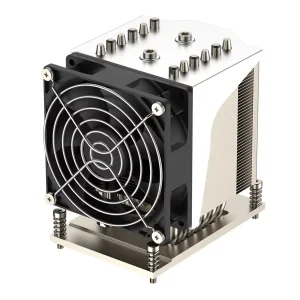
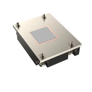
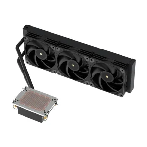
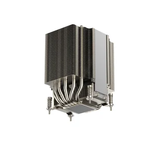
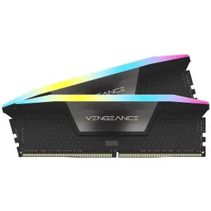
To combat high thermal dissipation requirements, we offer direct copper-based passive thermal heat sinks, vapor-chamber technologies, and multi-heat-pipe configurations. Our active and passive cooling solutions, such as the LGA1700/AM5 and 4U Server liquid-cooled systems, are developed to prevent localized thermal bottlenecks. Effective heat transfer prevents thermal drift in optical laser modules and prevents clock-cycle throttling in DDR4/DDR5 system memory modules.
Yes, our products are regularly customized and verified to meet different international standards. NexaRAM provides full traceability documents, compliance declarations (CE, FCC, RoHS, REACH), and undergoes strict quality control through our QC division. This guarantees smooth integration into systems bound for North America, Europe, Southeast Asia, and the Middle East.
By partnering with over 850 strategic raw material suppliers, chip set distributors, and component fabricators, NexaRAM retains a flexible purchasing advantage. Even during semiconductor material constraints, our long-term supply agreements and deep relationships with raw material suppliers ensure a stable production schedule for both memory components and custom optoelectronic PCBA builds.
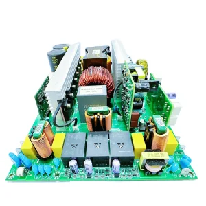
High-sensitivity assemblies must isolate tiny analog feedback signals from external noise. For gold metal detectors, this involves decoupling receiver coils with high-grade shielding and ground planes. In photovoltaic inverters, this translates to utilizing high-isolation optocouplers and power-management circuitry on the PCB assembly to handle high voltages while ensuring accurate signal feedback for stable grid synchronization.
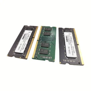
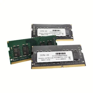
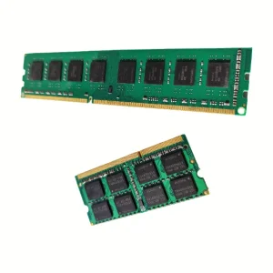
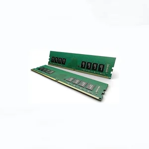
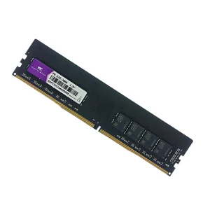
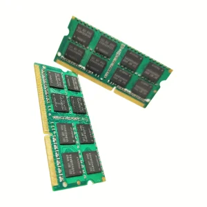
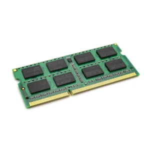
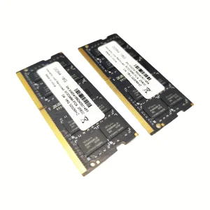
Each batch of DDR4/DDR5 modules undergoes a two-step validation process: Automated Optical Inspection (AOI) to inspect structural solder points, followed by a thermal-stressed burn-in chamber test run by our QC inspectors. These tests replicate high-stress server operational conditions to isolate and address component weaknesses before global shipment.