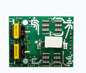
The global microelectronics and custom OEM Electronic Assembly Services market is experiencing a profound paradigm shift driven by the emergence of Artificial Intelligence (AI), high-performance computing (HPC), and next-generation memory protocols (specifically DDR5). No longer characterized merely by low-cost labor and routine component placement, contemporary electronic manufacturing demands an ecosystem-driven approach. OEMs and system integrators now prioritize end-to-end design-for-manufacturability (DFM), micro-precision surface mount technology (SMT), and high-integrity PCB routing that ensures signal propagation reliability in demanding environments.
In modern industrial and enterprise data applications, signal frequencies have entered the multi-gigahertz range, reducing the margin for error to near zero. A minor layout mismatch in a high-speed memory channel or an inadequate thermal dissipation plane in an enterprise server motherboard can compromise system stability. Consequently, leading microelectronics partners are transitioning toward specialized high-reliability facilities. These operations integrate real-time Automated Optical Inspection (AOI), automated 3D solder paste inspection (SPI), and high-temperature stress testing (burn-in testing) to achieve Defect-Free Manufacturing and secure operational integrity across automotive, cloud-computing, and telecom networks.
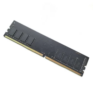
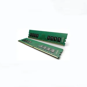
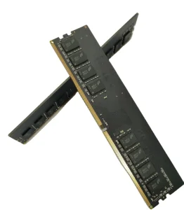
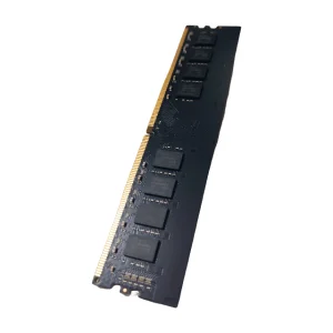
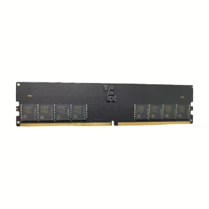
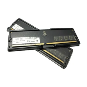
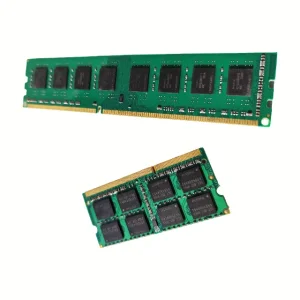
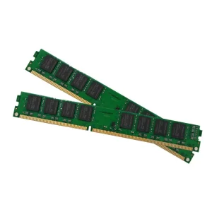
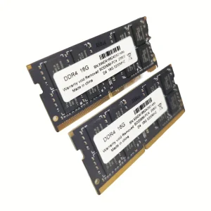
Established in 2016, NexaRAM Storage Technology Co., Ltd. is a professional DDR5 memory manufacturer specializing in high-performance RAM solutions for global OEMs, data centers, and enterprise computing applications.
Operating a modern production facility optimized for high-density configurations, NexaRAM leverages 6 years of direct export experience to serve systems integrators across North America, Europe, Southeast Asia, and the Middle East. Our core competence spans custom DDR5/DDR4 module design, PCB layout optimization, frequency tuning, and thermal solution development. Our dynamic engineering capability is evidenced by the release of 120 new product variants in the past year, ensuring clients maintain access to leading-edge specifications.
Under Google’s Search Quality Rater Guidelines, transparency in manufacturing facilities is critical to establishing Trustworthiness (E-E-A-T). Below is our certified testing, validation, and inspecting workflow.


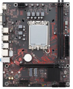
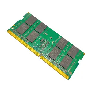
The integrity of custom electronic assembly relies heavily on engineering planning prior to reflow soldering. For devices utilizing modern chipsets, including Intel LGA1700 H610 architectures and high-density DDR4/DDR5 interfaces, layout strategies must balance electrical impedance targets against physical assembly limitations. Impedance target deviation by even 5% can induce signal reflections, degrade timing budgets, and create intermittent packet errors in enterprise systems.
Our engineering team leverages advanced simulation software to evaluate track routing, vias, and power distribution network (PDN) planes. In DDR5 routing, for example, the separation of address lines and command channels via precise trace geometries is critical. Spacing parameters must limit crosstalk to less than -35dB. Below is a structural outline of the primary considerations in our engineering and manufacturing sequence:
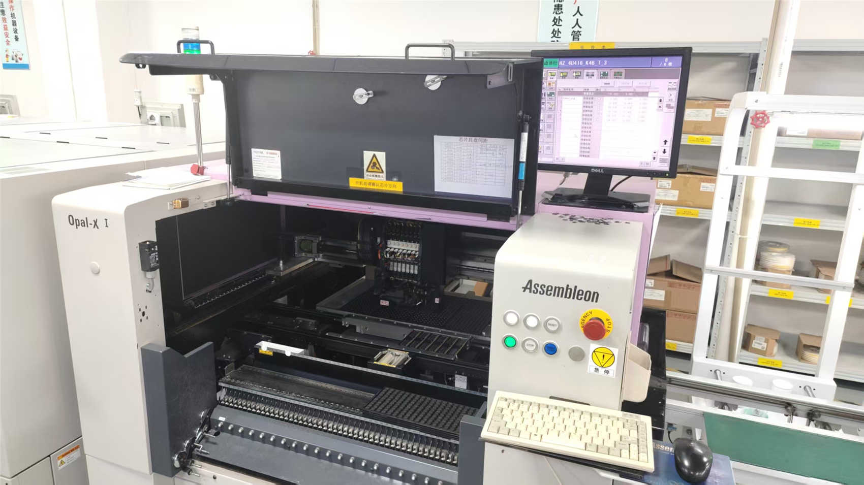
Implementing laser-cut stencils and 3D SPI (Solder Paste Inspection) ensures precise paste volume alignment on micro-BGA pads, eliminating bridges and voiding.
10-zone convection reflow ovens allow precise thermal gradient management, minimizing stress on fragile silicon substrates during lead-free SAC305 processing.
Integrated 3D AOI systems check placement accuracy, component orientation, and solder joint fillets against IPC-A-610 Class 3 workmanship criteria.
How we transform raw engineering drawings and component bills of materials (BOM) into certified, production-ready microelectronics.
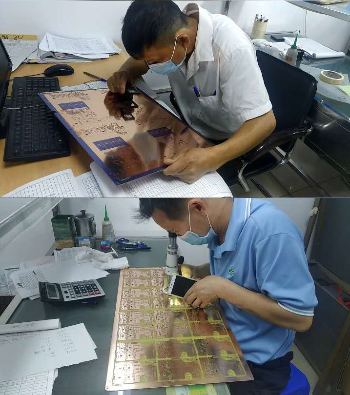
Every customer Gerber layout undergoes a comprehensive Design-for-Manufacturability inspection. In parallel, our simulation teams cross-reference PCB layer stackups with targeted trace impedances (typically 50-ohm single-ended / 90-ohm differential) to ensure high-speed transmission compatibility.
To prevent counterfeit components from entering production, all semiconductors, capacitors, and PMICs are sourced directly from verified primary fabricators or certified global distributors. We maintain full batch-code tracking across our 850 strategic supply chain partners.
Solder paste placement is verified using laser SPI. Components are mounted via automated high-speed chip shooters capable of handling 01005 passives and ultra-fine pitch BGAs. Temperature ramp-up, liquidus times, and cooling rates are monitored continuously in our nitrogen-purged reflow chambers.
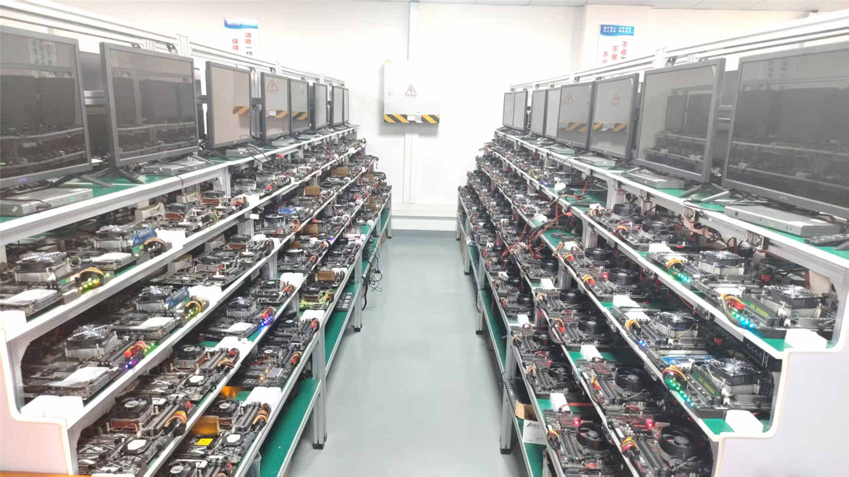
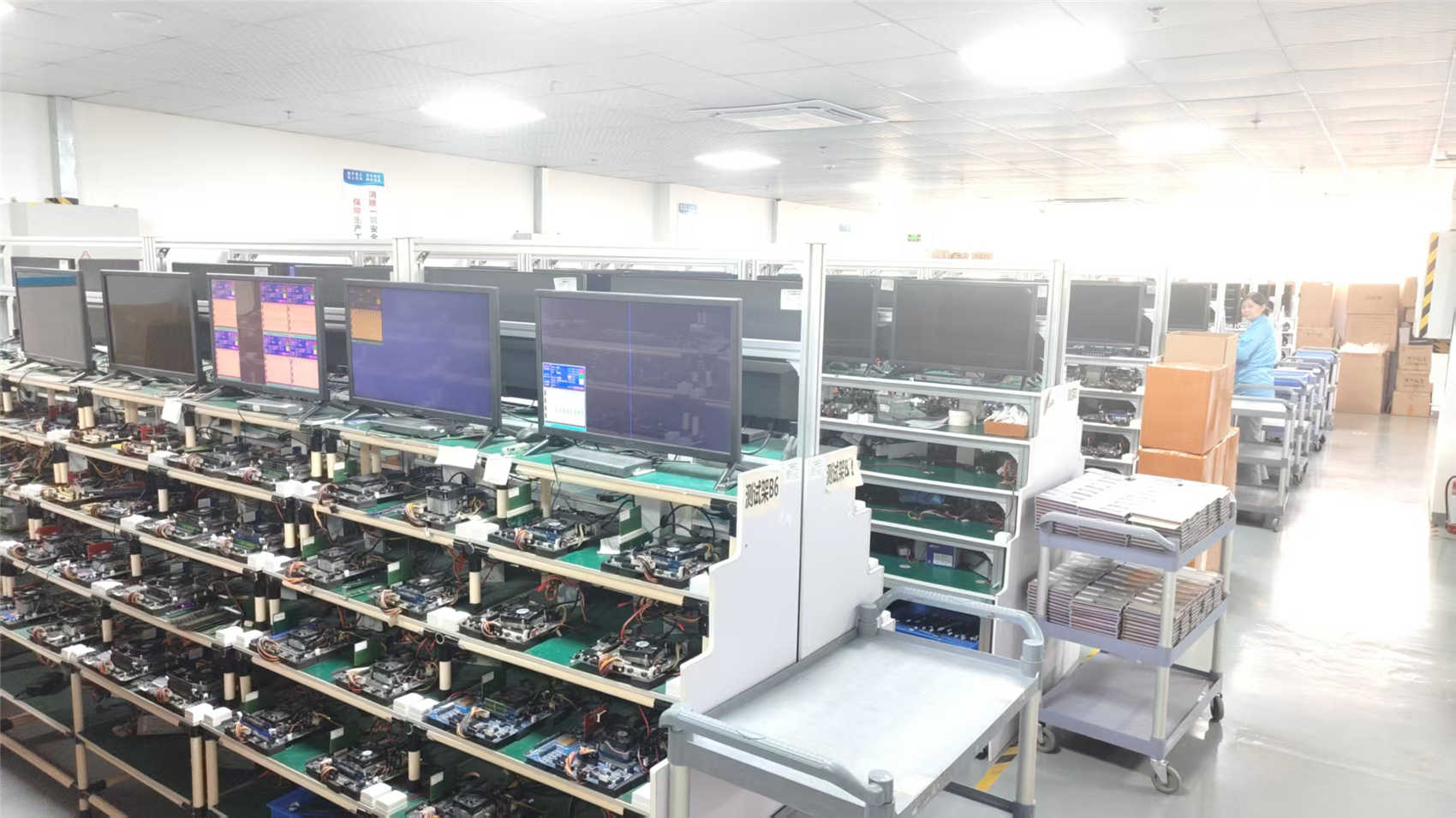
Post-assembly PCBA arrays undergo automated testing. For memory modules (DDR4/DDR5), this includes temperature-controlled thermal stress testing (burn-in) to screen out early-life failures. Physical validation is performed by our QC team of 35 dedicated inspectors.
Operating a global commercial footprint across North America, Europe, and Asia requires a thorough understanding of trade regulations, hardware compliance, and ecological directives. NexaRAM Storage Technology ensures that all custom electronic assemblies adhere strictly to global regulatory frameworks, reducing liability and friction for system integrators.
We manufacture in compliance with the RoHS (Restriction of Hazardous Substances) directive, ensuring that lead, mercury, cadmium, and hexavalent chromium levels stay below legal thresholds. This is critical for medical, industrial, and consumer markets. Additionally, our materials meet the European Union's REACH (Registration, Evaluation, Authorization and Restriction of Chemicals) framework to ensure chemical safety across the component lifecycle.
For electrical compliance, our assemblies are designed to pass CE (Conformité Européenne) and FCC (Federal Communications Commission) Part 15 Class A/B testing. This requires careful consideration of electromagnetic interference (EMI) shielding, proper PCB grounding design, and differential pair length matching to suppress unwanted emissions. By handling compliance engineering at the prototype stage, we protect our clients from costly product redesigns during compliance testing.
The future of electronic manufacturing lies in digital integration. At NexaRAM, we are laying the groundwork for a transition toward a fully unified, smart factory environment. This approach bridges ERP databases directly with line machinery to allow real-time adjustments and predictive maintenance.
Through machine learning models operating on AOI inspection data, our lines are becoming capable of predicting when component placing nozzle wear or solder paste viscosity changes might cause defects. By addressing variation before it leads to faulty boards, we target a first-pass yield (FPY) of 99.8%. Furthermore, as DDR5 memory modules evolve into higher clock rates, our development teams are already validating DDR6 physical layouts, focusing on advanced power distribution networks and noise isolation technologies.