Industrial-grade solutions powering advanced processing units and memory architectures
Key drivers behind high-density, multi-layer circuit development for modern electronics
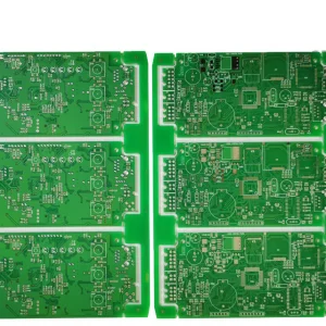
In the rapidly advancing digital age, printed circuit boards (PCBs) act as the central nervous system for everything from IoT smart devices to enterprise-class data centers. PCB rapid prototyping serves as the critical validation bridge, allowing hardware engineers to test complex trace layouts, signal integrity, and thermal mitigation schemes before proceeding to capital-intensive mass manufacturing.
Modern boards utilize blind and buried microvias to route signals on dense circuit configurations. Our analysis covers factories capable of routing line widths down to 2.5 mil for advanced computing chips.
For high-frequency standards like PCIe Gen 5/6 and DDR5 channels, strict control over material stackups (such as Megtron 6 or Rogers substrates) is critical to prevent insertion losses and reflections.
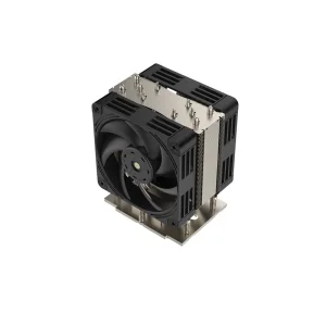
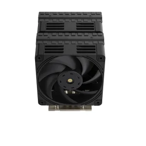
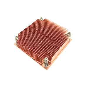
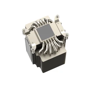
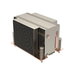
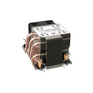
Increased component power demands, particularly from high-TDP server CPUs and server modules, require copper-clad or heavy-copper PCB cores, working alongside advanced CPU coolers for optimized operation.
A global compilation based on quality, technical limits, turn-around times, and customer reviews
Known for highly automated, ultra-low-cost, high-speed output. They process thousands of prototype orders daily, making standard double-layer and multi-layer boards accessible to engineers worldwide within a 24-48 hour window.
A comprehensive platform offering flexible, small-to-medium run PCBs alongside turn-key SMT assembly. Excellent for Rogers/Teflon high-frequency prototyping, advanced aluminum substrates, and flexible circuits.
A leading domestic provider in North America. Specializes in military-aerospace grade boards requiring ITAR compliance, DOD certification, and strict adherence to IPC Class 3 guidelines.
Renowned for state-of-the-art microelectronics fabrication, ultra-fine-pitch HDI boards, and signal integrity validation. Ideal for silicon validation boards and high-frequency testing fixtures.
The gold standard for European hardware developers. Focusing on high-quality DFM (Design for Manufacturability) verification software, ensuring boards run seamlessly on localized assembly lines.
A favorite among community makers and research labs for open-source hardware prototyping. Renowned for their signature purple solder mask, high-quality ENIG plating, and competitive batch pricing.
Specializes in multi-layer board systems and turn-key PCBA, offering full trace testing and component validation. Equipped to handle high-reliability projects for industrial control systems.
Utilizes intelligent collaborative manufacturing networks to optimize delivery speeds. Features specialized SMT rapid-prototyping lines catering to IoT and smart consumer devices.
Working in synergy with elite fabrication plants, this ecosystem delivers custom high-frequency multi-layer RAM substrate modules, optimized for high-speed signal pathways (up to DDR5 specifications) and advanced thermals.
A premium European manufacturer serving industrial automation, medical, and automotive sectors. Offers high-reliability prototyping with extensive consulting on electromagnetic compatibility (EMC) and thermal management. Ensures compliant and secure designs for mission-critical operations.
The Pearl River Delta (primarily Shenzhen and Guangzhou) remains the epicenter of the global electronics industry. For PCB fabrication and SMT component mounting, this cluster provides unparalleled advantages that cannot be easily replicated elsewhere.
Complete Bill-of-Materials (BOM) Convergence: Within a 50-kilometer radius, engineers can secure raw laminates, active integrated circuits, passive components, custom heat sinks, and enclosure plastics. This eliminates global shipping delays during crucial debugging cycles.
Advanced Automation & Scale: Modern Chinese factories have updated from labor-intensive assembly to fully automated operations featuring computer-controlled solder paste printers, high-speed pick-and-place equipment, and multi-zone reflow ovens. This enables cost-effective single-board runs and rapid transitions to volume production.
The engineering trajectory of printed circuits and high-performance computing systems
Traditional subtractive etching processes are reaching their limits. The industry is moving toward semi-additive processes (mSAP) that enable trace widths under 20µm, allowing dense routing next to high-pin-count BGA chips.
As transmission speeds climb, signal attenuation becomes a major design hurdle. Future PCB roadmaps emphasize ultra-flat copper foil treatments (to reduce skin effect loss) and ultra-low-loss dielectric materials.
To overcome traditional copper-routing bandwidth limits in data centers, future PCB technology will integrate optical waveguides directly into the substrate stack, enabling optical data transfers directly to the processor.
How prototype boards translate into specialized, real-world hardware systems
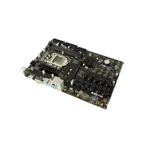
High-TDP processors (such as AMD SP5 or Intel LGA4677 sockets) require massive multi-layer motherboards capable of handling high thermal stresses. Specialized heavy-copper PCBs are coupled with active air and liquid cooling blocks to ensure stability.
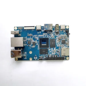
Complex SoCs like the Rockchip RK3588S feature integrated NPUs that demand precise power distribution networks (PDN). Prototyping ensures these compact multi-layer boards maintain signal integrity under fluctuating processing loads.
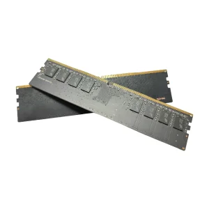
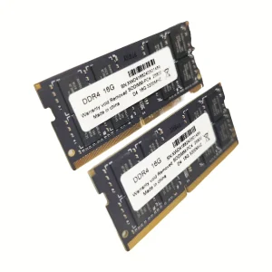
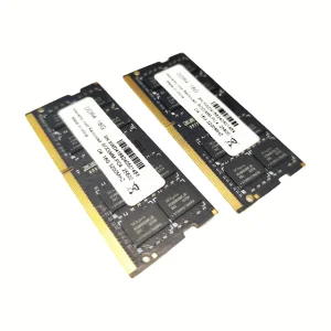
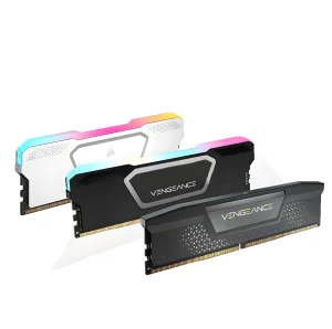
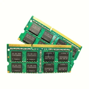
Modern memory systems run at high frequencies (e.g., DDR5 at 5200MHz+). Engineering prototypes require impedance-controlled routing, matched-length traces, and advanced layer stacks to mitigate crosstalk and electrical noise.
Established in 2016, NexaRAM Storage Technology Co., Ltd. is a professional DDR5 and DDR4 memory manufacturer specializing in high-performance RAM solutions for global OEMs, data centers, and enterprise computing systems.
We manage a modern production facility equipped with advanced manufacturing and testing systems to maintain stable, high-yield production capacities. Backed by 6 years of export experience and 12 years of industry experience in the memory and semiconductor sectors, NexaRAM maintains an annual export revenue of approximately USD 12 million.
Quality is controlled through a combination of automated optical inspection (AOI) and burn-in reliability testing, supported by a professional QC team of 35 inspectors. We work within a highly developed supply chain network of over 850 strategic partners to ensure stable sourcing of high-grade components.
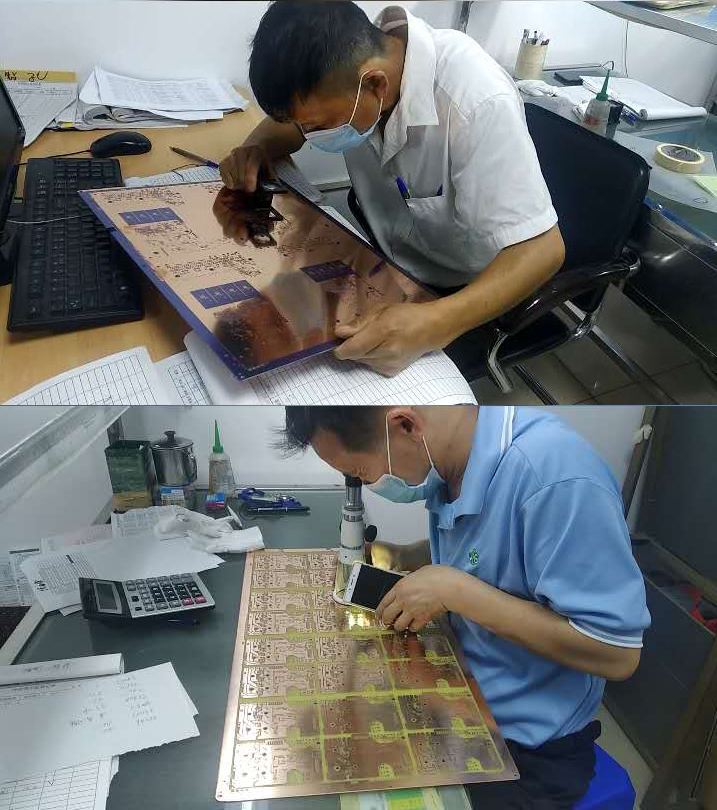
 DRAM Inspection Process
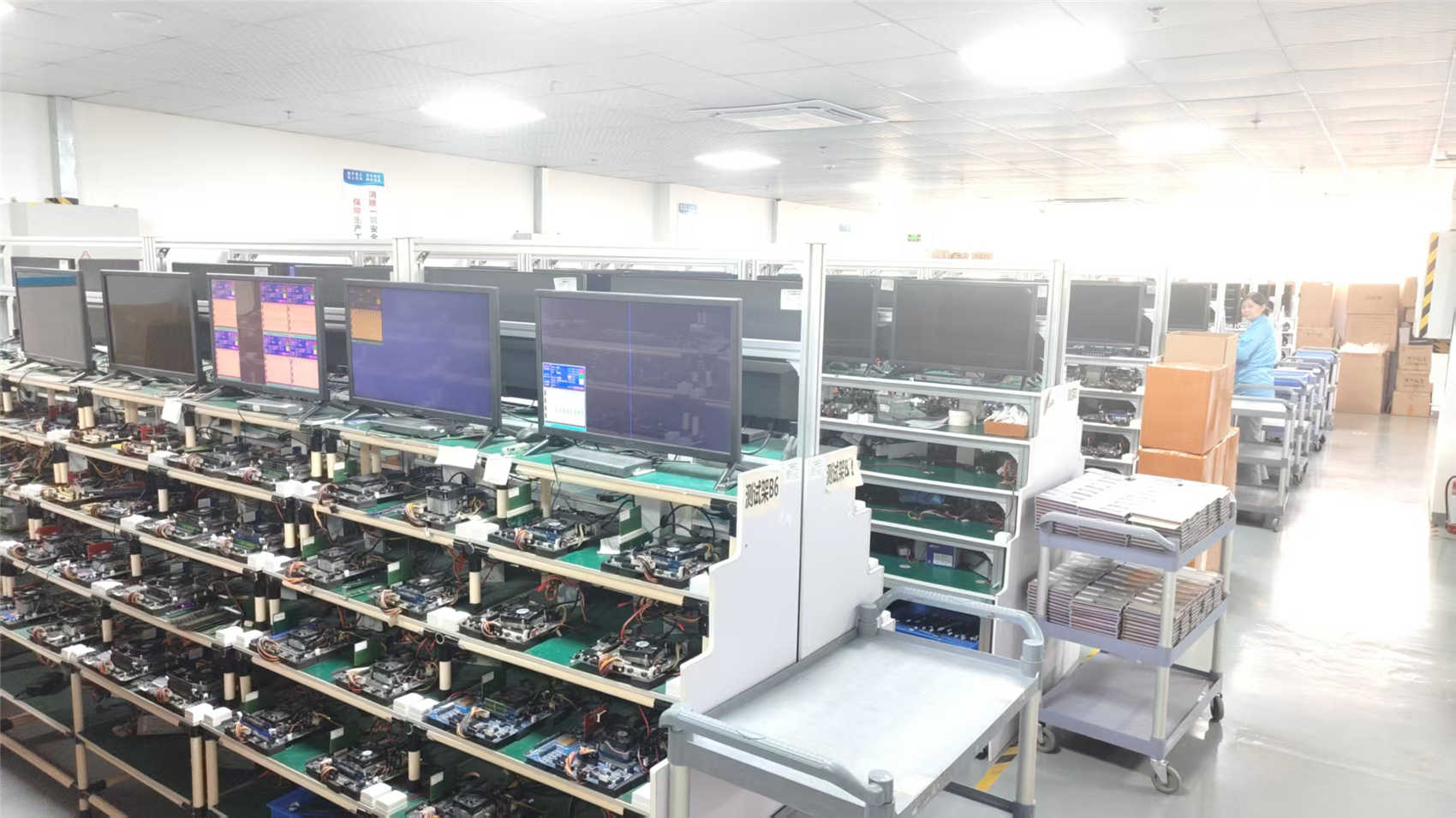 High-Speed Testing Jigs
 DDR5 Validation Platform
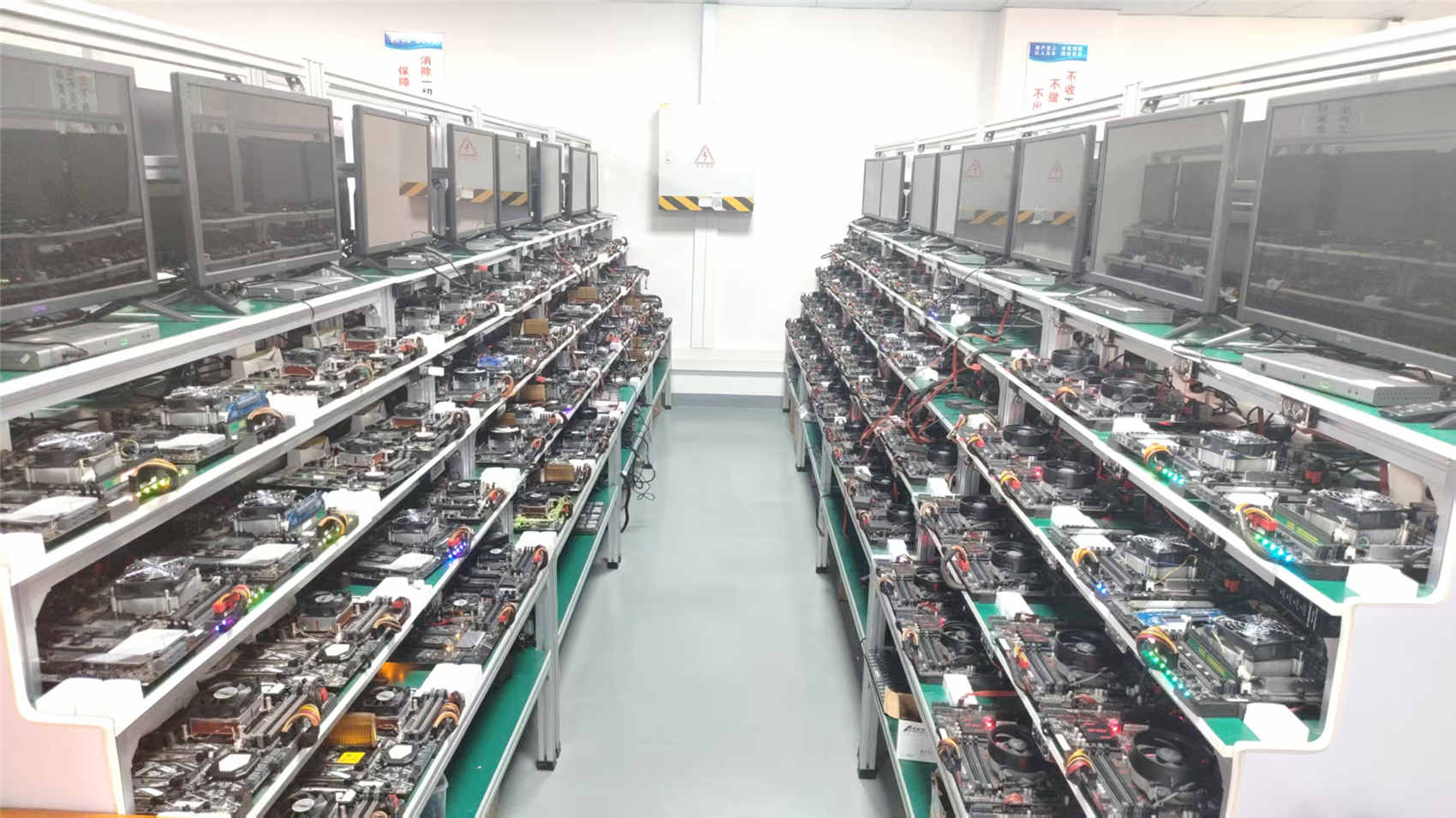
 Semi-Automated Assembly
 Burn-In Stress Testing Room
 Quality Control Center
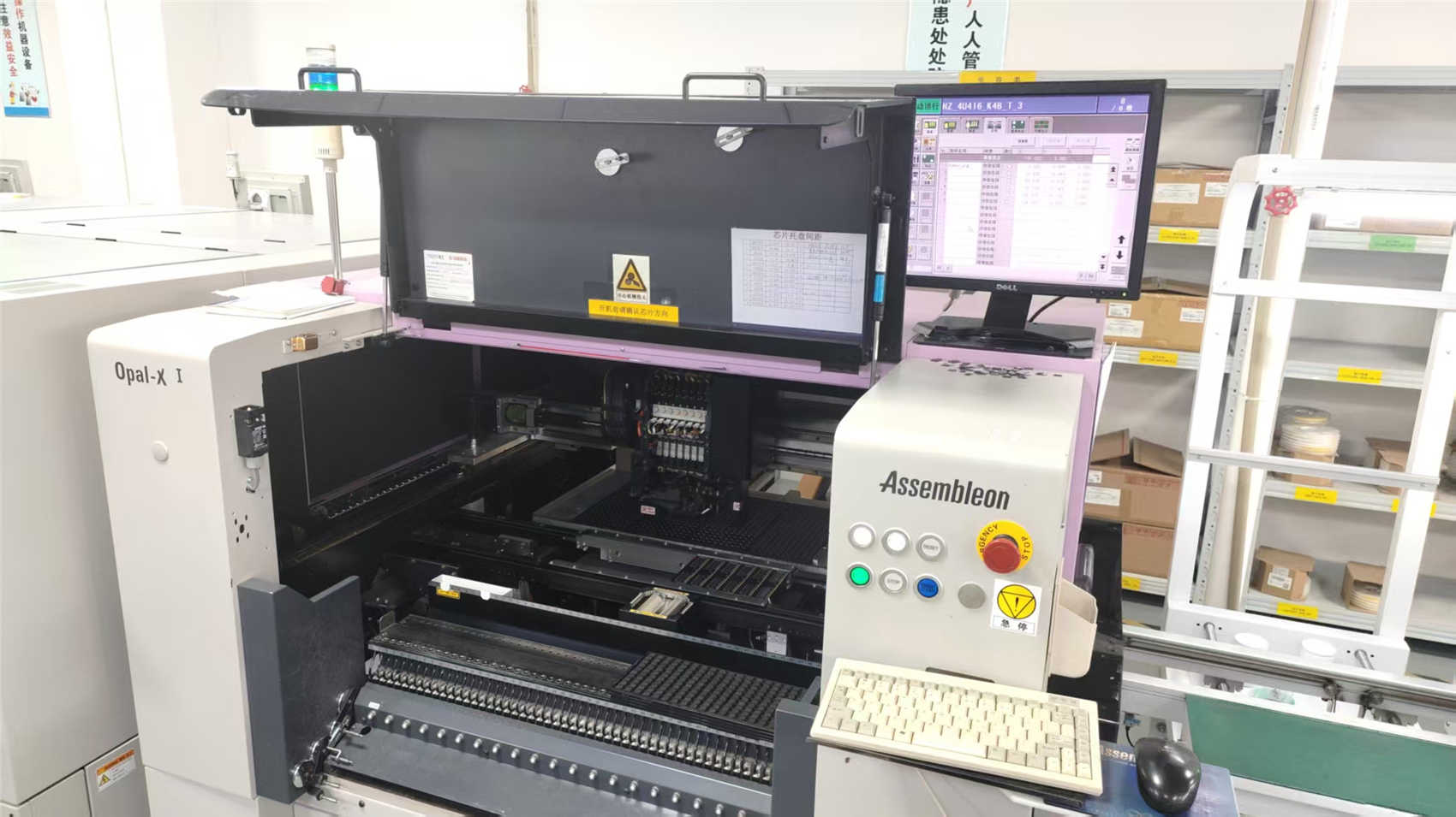
 Enterprise SMT Line and High-Speed Placement Assembly System
Ensuring design compliance across global regulatory frameworks
When delivering PCB prototypes and finished memory modules to international markets (including North America, Europe, Southeast Asia, and the Middle East), compliance with local directives is essential.
In addition to international certifications, having local technical representatives helps streamline communication. Regional engineers can assist with impedance calculations, resolve DFM issues, and verify localized mechanical constraints (such as heat sink clearances and connector layouts). This helps avoid design iterations, saving time and resources.
Expert insights on PCB prototyping, manufacturing capabilities, and hardware validation
Complete your hardware setup with our specialized cooling, memory, and controller modules