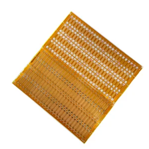
Advanced high-sensitivity substrates, polyimide flex modules, and high-frequency laminates optimized for the Kansai region's elite manufacturing networks.
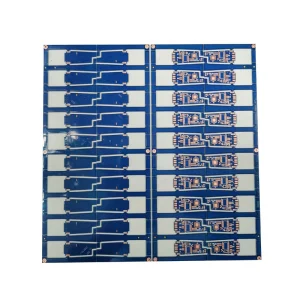
Osaka and the broader Kansai region have long served as the heartbeat of Japan's precision engineering, electromechanical, and heavy industrial output. Unlike other manufacturing hubs globally that focus solely on low-cost high-volume fabrication, Osaka's manufacturing matrix specializes in high-mix, low-to-medium volume production characterized by extremely tight tolerances, advanced substrate research, and unmatched quality control. Local PCB factories in Higashiosaka and Kadoma are embedded in a tight-knit ecosystem of specialized chemical processors, micro-drilling experts, and substrate laminators.
For global procurement teams, sourcing single-sided and double-sided PCBs from Osaka offers structural reliability that cannot be matched by commodity-grade manufacturers. Single-sided boards serve essential roles in high-power industrial control panels, white goods, and primary power distribution blocks where dielectric isolation and track cross-sections must remain stable under thermal loads. Meanwhile, double-sided PCBs act as the foundational architecture for complex control circuits, medical apparatus instrumentation, automotive lighting, and intermediate power converters. This regional focus ensures that even basic boards benefit from ultra-pure copper foil deposition, advanced photoresist coatings, and premium surface finishes (such as Electroless Nickel Immersion Gold - ENIG).
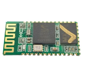
Established in 2016, NexaRAM Storage Technology Co., Ltd. has developed into a reliable manufacturer in the DRAM, advanced semiconductor module, and specialized PCB substrate sectors. NexaRAM operates a high-precision testing facility with a building area of approximately 320㎡, optimized for rapid iteration, inspection, and verification of complex circuit configurations. With 12 years of industry experience in memory and semiconductor-related fields, alongside 6 years of global export experience, the company maintains an annual export revenue of USD 12 million.
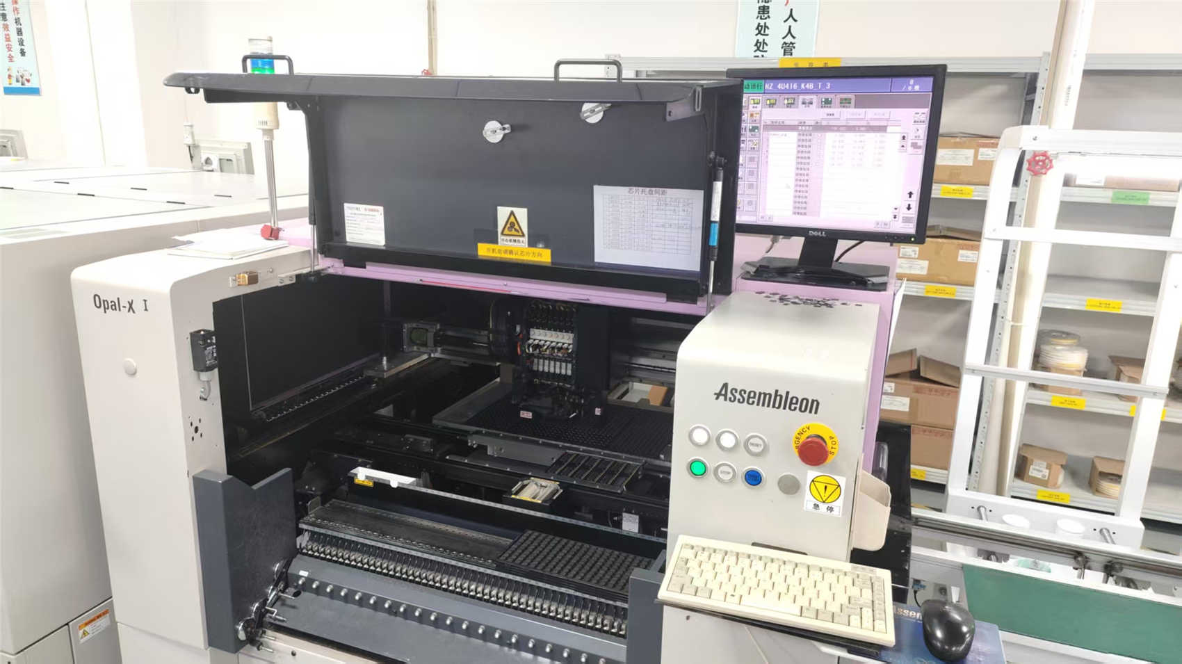
This facility is designed around a fully automated surface-mount technology (SMT) ecosystem and strict optical inspection nodes. Sourcing directly through NexaRAM allows clients to access a supply chain supported by over 850 strategic partners, securing premium Grade-A silicon, specialized substrates, and rare copper laminates even during volatile supply periods. NexaRAM’s engineering capabilities bridge the gap between memory substrate design and general PCB production, enabling custom layout optimizations, trace width matching, and thermal solution modeling for both consumer and high-reliability industrial projects.
Designing circuits for harsh electromagnetic or thermal environments requires a granular understanding of substrate mechanics. The selection between single-sided and double-sided structures dictates the board's routing density, impedance consistency, and dissipation pathways.
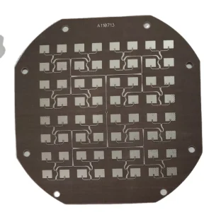
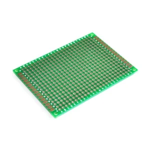
Single-Sided PCBs (SS-PCBs): Consisting of a single conductive copper layer laminated onto a non-conductive core material (such as FR-4, CEM-1, or Aluminum), these boards utilize one side for traces and the other for component mounting (primarily through-hole). SS-PCBs manufactured under Osaka-grade guidelines focus on trace adhesion, surface finish flatness, and high dielectric strength. They are widely used in cost-critical, high-current applications, such as LED light engines and basic power supply modules.
Double-Sided PCBs (DS-PCBs): These designs utilize copper cladding on both sides of the substrate core, allowing for routed connections on both layers. Communication between the top and bottom layers is established using Plated Through-Holes (PTH) or microvias. This layout dramatically increases routing flexibility and component density, enabling differential pairs to be routed over solid ground reference planes—a vital prerequisite for noise reduction in communications and memory devices.
| Feature / Parameter | Single-Sided PCBs | Double-Sided PCBs | High-Frequency Substrates (e.g., Taconic) |
|---|---|---|---|
| Layer Count | 1 Layer (Single copper foil) | 2 Layers (Double copper foils) | 1 or 2 Layers (Substrate optimized) |
| Routing Density | Low (Strictly planar traces) | Medium-High (Inter-layer vias) | High (Matched impedance traces) |
| Primary Dielectric Core | FR-4, CEM-1, Aluminum back | FR-4, High-Tg FR4, Polyimide | Taconic TLY-5, PTFE, Ceramic |
| Typical Solder Mask | Liquid Photo Imageable (LPI) | Liquid Photo Imageable (LPI) | Low-Loss Solder Mask or Maskless |
| Common Surface Finishes | HASL, Lead-free HASL, OSP | ENIG, Immersion Silver, HASL | ENIG, ENEPIG (for wire bonding) |
| Primary Application Area | Power supplies, LED modules, Toy circuits | Industrial sensors, Memory cards, Keyboards | RF Transceivers, Radars, High-speed Telecom |
Modern SMT lines are shifting toward hybrid designs, where double-sided PCBs incorporate high-performance cores, such as Taconic TLY-5 (dielectric constant $D_k \approx 2.2$, dissipation factor $D_f \approx 0.0009$). These materials are essential for RF and high-frequency communication boards where signal loss must be kept near zero, allowing Osaka-made boards to operate seamlessly in demanding high-frequency equipment.
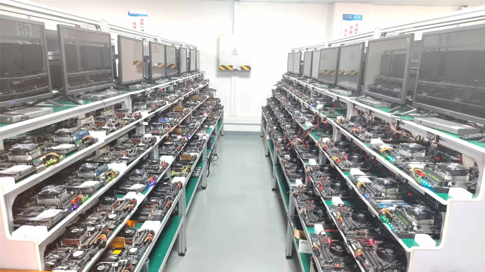
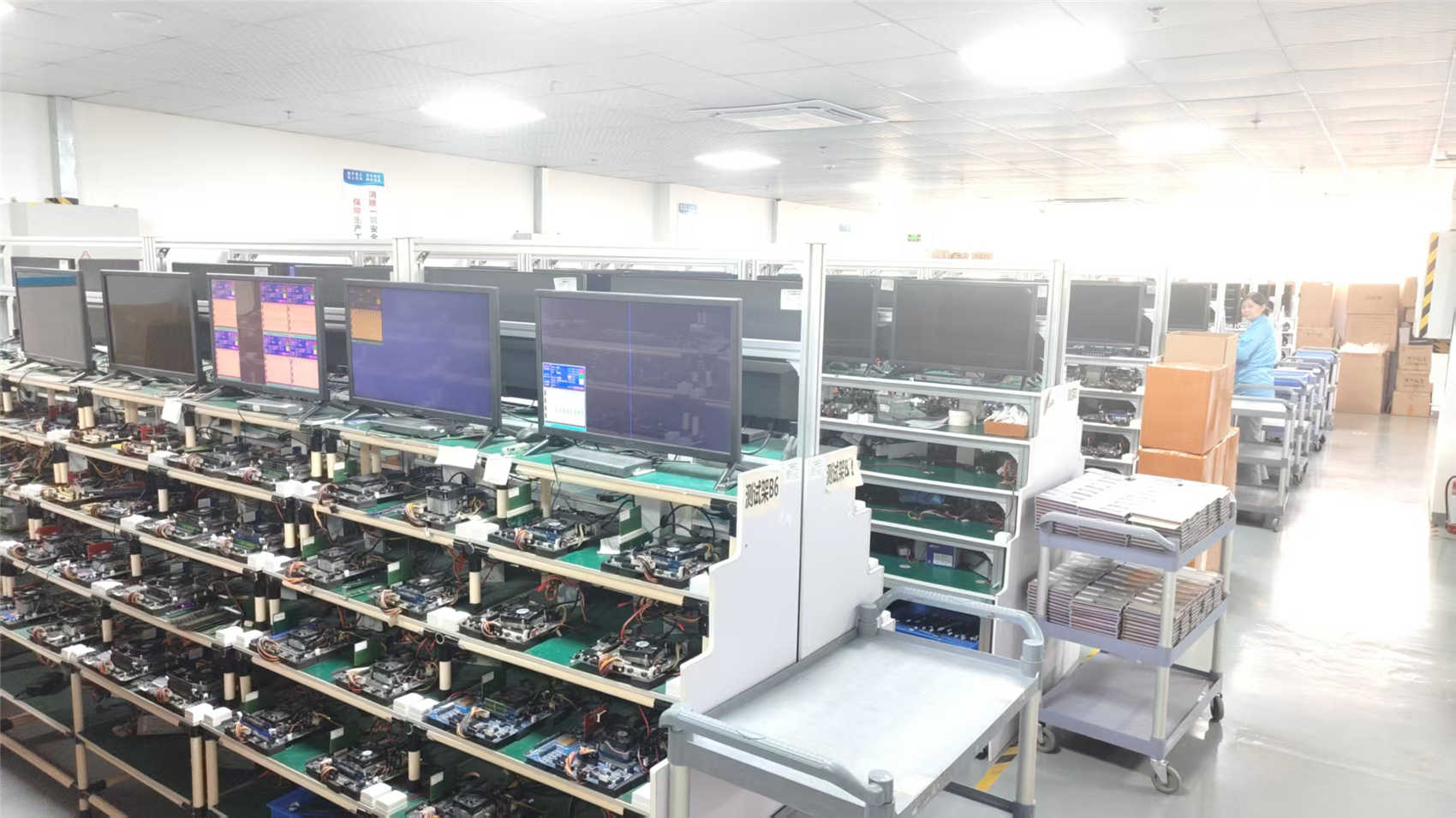
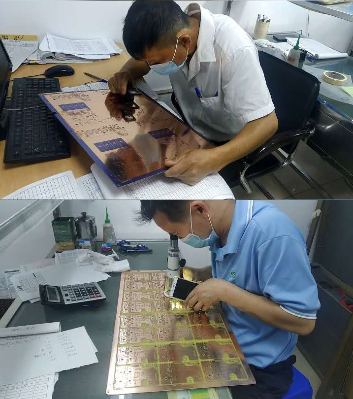
At NexaRAM's modern facility, quality is managed using multi-stage inspection lines. The production sequence relies on an expert quality control department comprised of 35 dedicated QC inspectors who monitor board fabrication, component sourcing, and SMT assembly. Each production batch undergoes testing protocols designed to identify micro-fractures, delamination, track impedance variations, and cold solder joints before packaging.
The inspection process is anchored by two critical validation methods:


By maintaining clear records for every batch, NexaRAM complies with global regulatory mandates and industrial expectations. This level of quality control guarantees that boards shipped to North America, Europe, Southeast Asia, and the Middle East are ready for integration without requiring additional local QA testing.
Modern electronics require a balanced design approach where the PCB layout and thermal solutions work together seamlessly. As microprocessors and memory modules run at higher clock speeds, thermal dissipation becomes a primary limiting factor.
NexaRAM addresses these challenges through integrated, system-level design solutions:
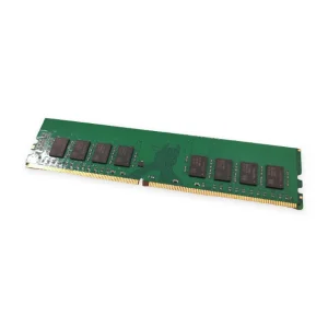
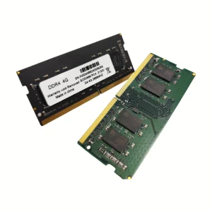
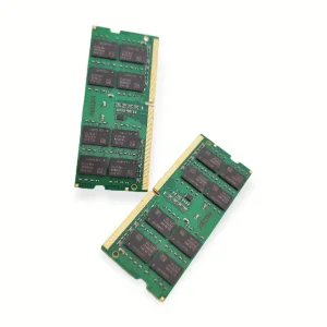
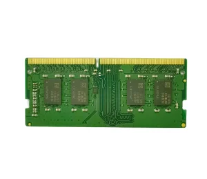
The industry transition from DDR4 memory systems to high-speed DDR5 architectures highlights the shifting demands on PCB substrates. While DDR4 operates at speeds up to 3200 MT/s, DDR5 begins at 4800 MT/s and scales beyond 6000 MT/s. This performance increase requires significant changes in substrate engineering:
Talk to our engineering team to optimize your PCB layout, thermal management systems, or high-speed memory modules.
Inquire About Custom EngineeringOsaka-based factories specialize in high-mix, precision-engineered production runs. By sourcing through this Kansai manufacturing cluster, buyers gain access to ultra-pure copper deposition, advanced photoresist chemistry, and strict quality control. This is critical for applications that require long-term reliability in harsh environments, such as automotive systems or industrial sensors.
We use a multi-stage inspection flow that combines automated optical inspection (AOI) with burn-in reliability testing. Our 35-person quality control department monitors every stage from raw substrate inspection to final assembly, ensuring all boards meet international compliance standards.
For high-frequency applications, we use low-loss laminates like Taconic TLY-5 (0.254mm thickness) which feature a low dielectric constant. For high-temperature setups, we utilize aluminum substrates or high-Tg FR-4 cores that provide excellent thermal dissipation.
Yes. Backed by our R&D team of 180 engineers, we offer comprehensive layout design, impedance modeling, and frequency tuning. We ensure that your memory substrates, mainboards, and high-frequency PCBs are optimized to prevent signal loss and crosstalk.
Yes. All raw materials, copper foils, solders, and surface finishes used in our production lines comply with RoHS, REACH, and lead-free directives, ensuring trouble-free importation into North American and European markets.
Standard prototypes are typically completed in 5 to 7 working days. Mass production runs usually require 15 to 20 working days, depending on material complexity, layer count, and SMT assembly requirements.
Yes. We design and supply matching thermal solutions, including LGA server coolers, direct-contact heat pipes, and integrated liquid cooling plates, to match the power requirements of your board layouts.
MOQs vary based on design complexity. For standard single and double-sided PCBs, we support low prototyping volumes (10-50 units). For complex memory modules or custom multi-layer SMT designs, MOQs are negotiated based on tooling setup requirements.
Premium prototype breadboards, enterprise cooling platforms, and high-performance DDR4/DDR5 system memory modules built to meet strict industrial tolerances.
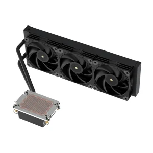
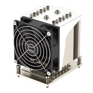
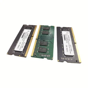
We also design, manufacture, and distribute specialized server-grade thermal hardware and memory substrates for performance computing:
Whether you require high-frequency aluminum substrates (Taconic TLY-5), standard double-sided prototyping runs, or advanced memory module manufacturing, our team delivers the engineering precision your projects demand.
Send Inquiry Now