New York is rapidly evolving into a pivotal hub for advanced hardware engineering, defense electronics, aerospace technologies, and high-frequency financial trading systems. From the tech innovation corridors of NYC to the semiconductor research centers upstate, local system integrators require exceptional precision and fast-turn prototyping capabilities. The complexity of modern applications demands a paradigm shift away from basic, dual-layer layouts toward dense, multi-layer circuit boards capable of routing gigahertz-speed signals while maintaining extreme thermal stability.
"In high-speed computing and mission-critical electronics, signal degradation, crosstalk, and thermal management are the primary bottlenecks. Multi-layer structures with custom stack-ups are no longer optional—they are the foundational baseline of robust system architecture."
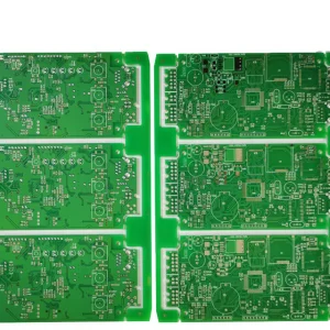
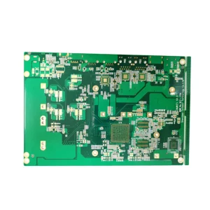
As a premier export partner and tech consultancy, we bridge the gap between regional design teams and advanced global manufacturing. Our capabilities support complex multi-layer configurations (up to 32 layers) using high-Tg materials, controlled impedance matching, and blind or buried via geometries, guaranteeing that regional designs translate directly into yield-ready, production-grade components.
While domestic fabricators in the New York metropolitan area provide rapid local prototyping, volume production requires a reliable global logistics network to maintain cost-efficiency. Our dynamic operational model pairs local New York technical support, engineering compliance review, and field application engineering (FAE) with our high-volume, automated production lines. This allows companies in Rochester, Buffalo, Syracuse, and Long Island to access ultra-modern manufacturing technologies without sacrificing localized communication or technical reassurance.
To keep pace with the demands of AI computing, server infrastructure, and next-generation signal speeds, our PCB manufacturing lines support a comprehensive matrix of materials, tolerances, and design geometries. Below is an overview of our core capabilities tailored for advanced project requirements.
| Parameter | Standard Capability | Advanced / Custom Tolerance |
|---|---|---|
| Layer Count | 2 to 16 Layers | 18 to 32+ Layers (High-aspect ratios) |
| Base Laminates | FR-4 (High-Tg, Mid-Tg), Lead-Free Compatible | Rogers, Megtron 6, Taconic, Teflon, Nelco |
| Dielectric Constants (Dk) | 3.8 to 4.6 | 2.2 to 3.5 (Low-loss, ultra-high speed) |
| Min. Trace Width / Space | 3.5 mil / 3.5 mil | 2.5 mil / 2.5 mil (HDI micro-routing) |
| Controlled Impedance | ± 10% | ± 5% (Precision differential pairs) |
| Surface Finishes | HASL (Lead-Free), OSP, ENIG | ENEPIG, Hard Gold, Immersion Silver/Tin |
| Via Technology | Through-hole, tented/plugged vias | Blind, Buried, Microvias (Laser-drilled), Via-in-Pad |
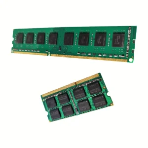
In high-frequency transmission environments, such as server motherboards and high-speed storage channels, impedance variance leads to signal reflections, bit errors, and EMI issues. Our engineering team uses advanced polar impedance solvers to run pre-stack-up simulations. By carefully adjusting copper thickness, track geometry, and dielectric spacing, we ensure that differential pairs are tightly matched, maintaining perfect signal integrity across high-speed interfaces like PCIe Gen 5/6, DDR5 memory, and 100G Ethernet channels.
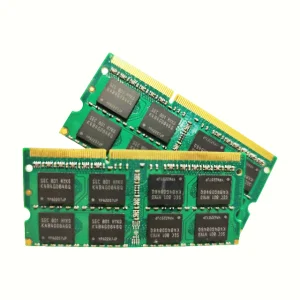
As a key manufacturing and semiconductor packaging partner, NexaRAM Storage Technology Co., Ltd. brings top-tier engineering resources, advanced quality control, and supply chain security to high-speed electronics projects.
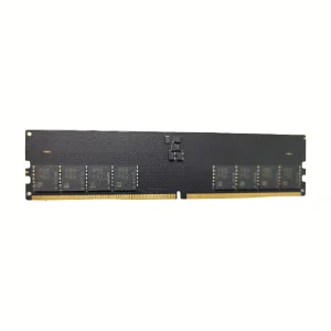
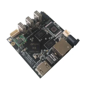
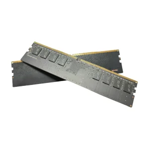
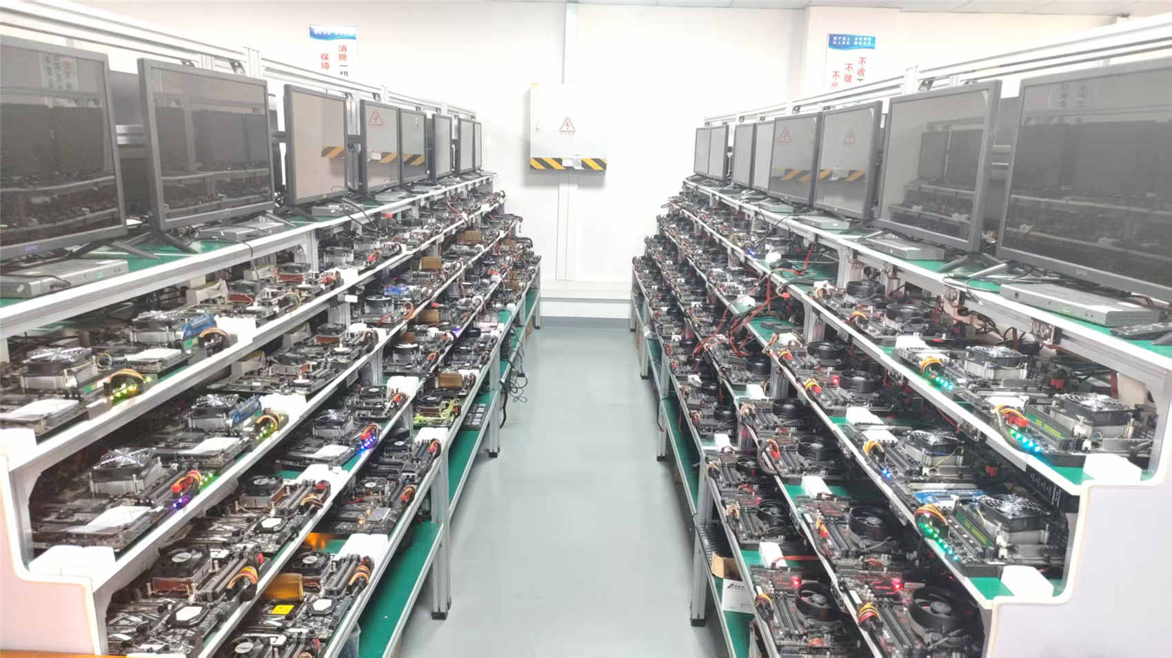
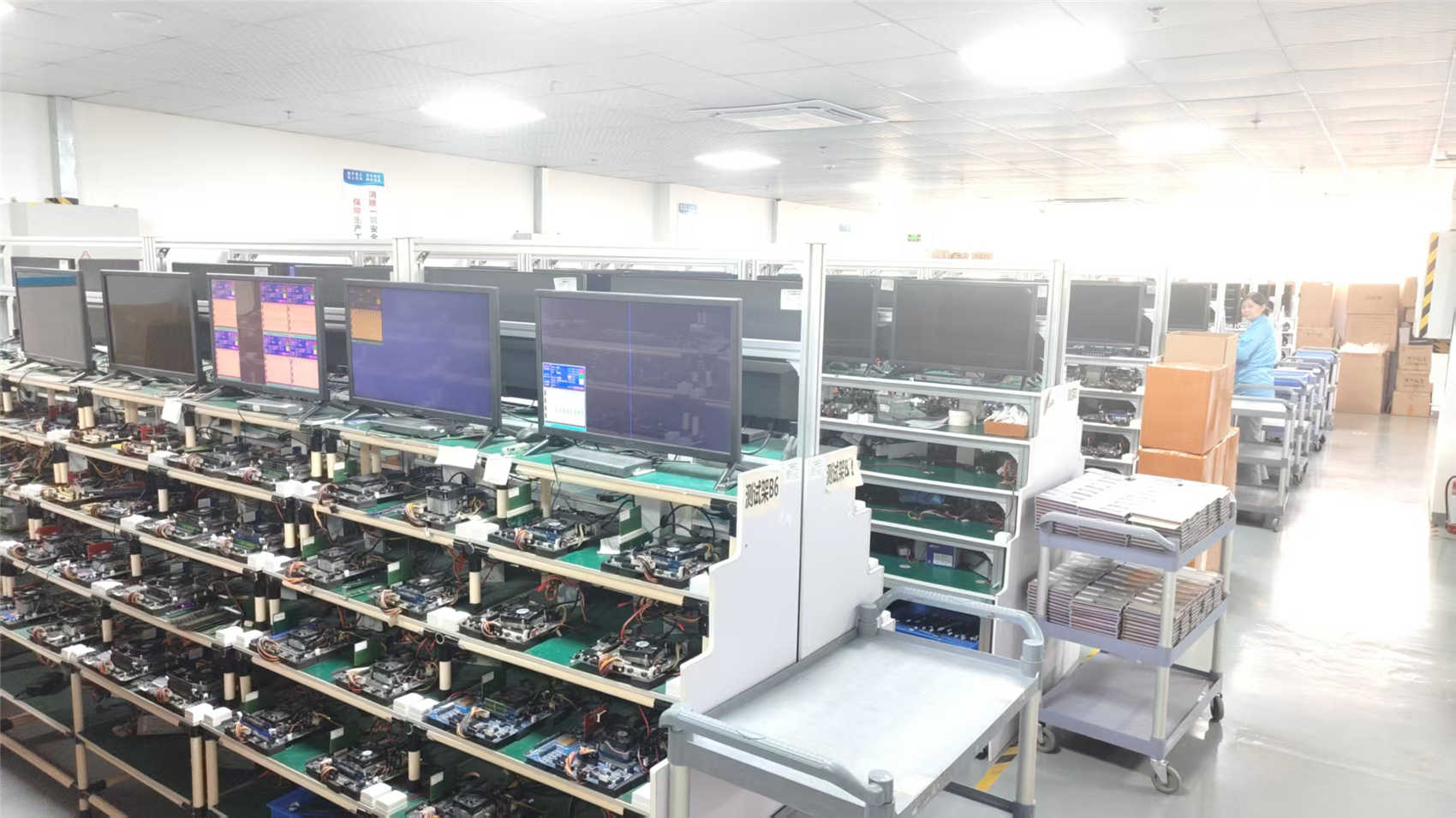
Founded in 2016, NexaRAM has expanded its footprint to become a reliable supplier in high-speed DRAM modules, semiconductor storage assemblies, and complex PCB fabrication. With an annual export revenue of USD 12 million and 6 years of export experience, our organization is structured to serve global OEMs, data centers, and advanced aerospace system integrators. Our modern facility features high-precision surface mount (SMT) lines, specialized testing jigs, and cleanroom environments, ensuring every batch complies with international standards.

The global electronics supply chain demands both agility and economic viability. By positioning our primary high-volume manufacturing assets within key industrial parks in China, we leverage a highly mature component ecosystem. With more than 850 strategic supply chain partners, we source raw copper laminates, specialized prepregs, and advanced components quickly, insulating our production schedules from material shortages.
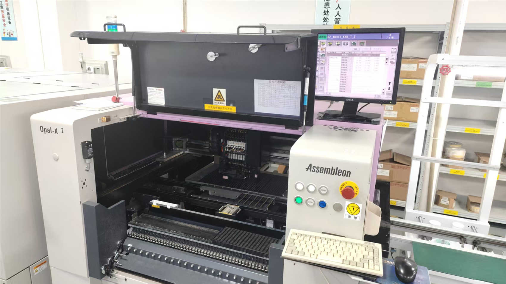
Our factories operate under strict Industry 4.0 guidelines. SMT placement machines, multi-stage reflow ovens, and Automated Optical Inspection (AOI) lines are interconnected via custom MES software, allowing for complete trace history of each manufactured batch.

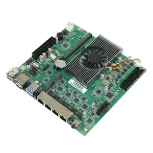
Advanced multilayer PCBs act as the central nervous system for modern high-reliability systems. Our engineering frameworks are custom-tailored for several critical industries in New York and globally:
Optimized stack-ups featuring ultra-low-loss dielectric materials (e.g., Megtron 6) and heavy copper layers to support DDR5/DDR6 signaling and high-power delivery architectures without signal degradation.
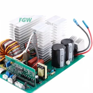
Ruggedized configurations built to handle harsh environments, wide temperature ranges, high vibration, and continuous power load demands typical in industrial welding and energy conversion.
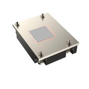
High-Tg substrate materials combined with immersion gold or ENEPIG surface finishes, guaranteeing long operational lifespans and zero failure rates under extreme thermal stress.
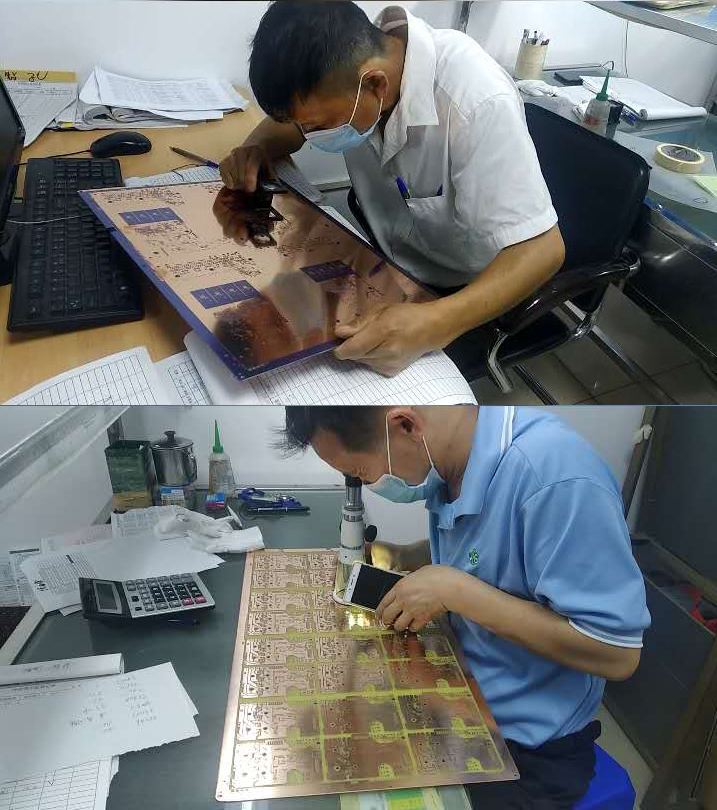
To meet the high standards of aerospace, defense, and medical markets in the United States, our manufacturing facility enforces strict quality control steps. Every batch undergoes rigorous inspection to ensure structural integrity and component functionality.
Our dedicated 35-inspector Quality Control team oversees automated optical inspection (AOI), X-ray material scanning, and automated functional tests. By using standardized testing frames, we ensure that multilayer alignment matches the original CAD files before shipping.


Partner with our engineering team to secure your global supply chain, optimize design stack-ups for signal integrity, and scale your production with NexaRAM's manufacturing infrastructure.
Send Inquiry NowWe use polar impedance calculation software to simulate trace behavior before production begins. Designers supply target impedance values (typically 50-ohm single-ended or 90/100-ohm differential). We optimize the stack-up (prepreg/core thicknesses and dielectric properties) to match your target tolerances within ±10% standard, or ±5% for highly specialized runs. We also run coupon tests on every manufacturing panel to verify trace parameters.
For standard operating designs up to 130°C, standard FR-4 is suitable. For higher operating temperatures, we recommend High-Tg FR-4 (Tg 170°C or 180°C). For high-frequency layouts running past 10 GHz, low-loss materials like Rogers, Taconic, or Megtron 6 are ideal. They feature a low dissipation factor (Df) to minimize signal losses and preserve transmission path integrity.
Yes, our plant is fully equipped for High-Density Interconnect (HDI) production. We use high-precision laser-drilling systems to make microvias down to 3-4 mils, supporting complex sequential lamination steps. Additionally, we support via-in-pad plating (VIPPO) technology, allowing designers to route interconnects directly underneath BGA pads to save board real estate.
Our strategic production assets are certified under ISO 9001:2015 for quality management systems. Furthermore, our multilayer production paths are compliant with IPC-A-600 and IPC-A-610 standards (Class 2 and Class 3 guidelines), UL-approved (Underwriters Laboratories), and compliant with RoHS regulations.