High-performance PCB assemblies and specialized board fabrications engineered to match local standards.
Singapore’s relentless drive toward Smart Nation 2030, automation, and advanced manufacturing has transformed the island’s electronics sector. High-reliability printed circuit boards (PCBs)—ranging from foundational single-sided boards used in consumer appliances to highly complex double-sided and multilayer substrates utilized in data hubs and automation systems—act as the bedrock of local product design, IoT infrastructure, and industrial computing platforms.
Whether deploying low-loss RF antennas, high-intensity LED systems, or complex robotics controllers in the Jurong Innovation District (JID), hardware engineers demand boards with exceptional thermal stability, strict mechanical tolerances, and unyielding quality verification. NexaRAM Storage Technology Co., Ltd. addresses this demand by pairing modern, certified production ecosystems with rapid shipping lanes straight to Singapore's tech hubs.
Key sectors fueled by our double and single-sided designs include:
Engineered to meet IPC-A-600 and IPC-A-610 Class II/III standards, ensuring exceptional mechanical and thermal performance.
We process standard FR-4 (Tg 130°C to 180°C), halogen-free laminates, aluminum-backed cores for thermal dissipation (up to 3.0 W/m-K), and high-frequency materials such as Taconic TLY-5 and Rogers formulations to handle up to 70GHz applications.
Supporting trace width and clearance down to 3 mil (0.075mm) for high-density interconnect designs. Microvia drills down to 0.15mm via mechanical drilling, and laser direct imaging (LDI) for sharp trace definition and minimal impedance fluctuation.
Ensuring flat pad geometries and robust shelf-life under humid environments: Electroless Nickel Immersion Gold (ENIG), Hot Air Solder Leveling (HASL Lead-Free), Organic Solderability Preservatives (OSP), and Immersion Silver/Tin.
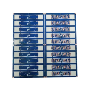
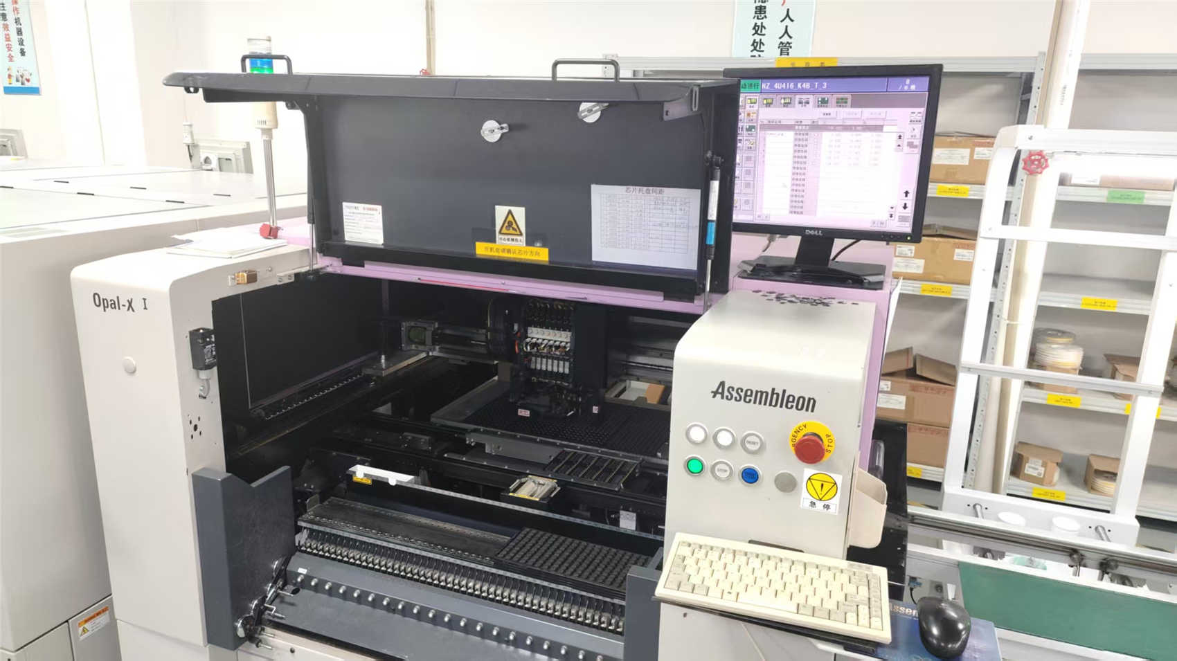
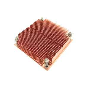
A snapshot of NexaRAM's partner production lines, advanced inspection, and test equipment ensuring zero-defect output for Singaporean clients.
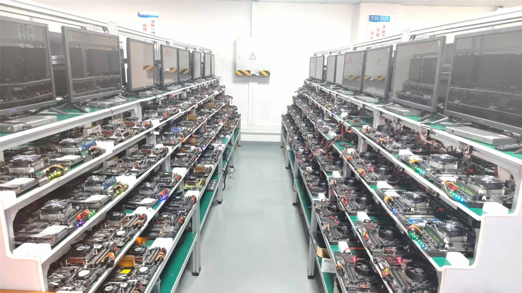

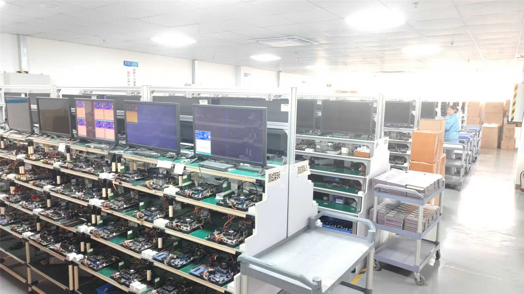


Operating a production center with 35 dedicated quality inspectors and 180 expert R&D engineers, NexaRAM Storage Technology Co., Ltd. builds high-yield platforms from single-sided mechanical assemblies up to complex double-sided and multilayer printed circuit boards. By utilizing more than 850 strategic supply chain partners, we secure cost advantages and high-purity laminates, passing the savings and speed directly to Singapore's fast-moving product teams.
We understand that lead times dictate product launch cycles. Our localized support pipeline ensures that Singapore engineering houses receive DFM (Design for Manufacturing) reports within 12 hours of Gerber submittal. Airfreight channels from Shenzhen and Guangzhou straight to Changi Airfreight Centre (CAC) allow us to offer 3-day turnaround prototypes and 7-to-10 day bulk production deliveries, bypassing traditional supply chain bottlenecks.
Singapore Compliance & Standards: We ensure that every batch of single or double-sided PCBs shipped to the Singapore market meets the requirements of RoHS, REACH, UL 94V-0 flammability ratings, and aligns with environmental guidelines outlined by the National Environment Agency (NEA) and IMDA standards.
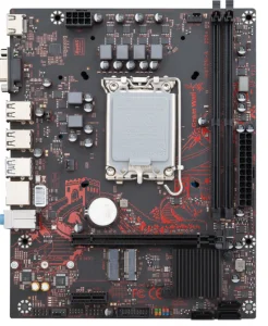
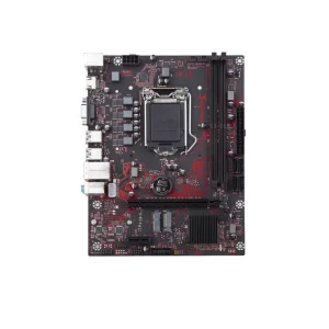
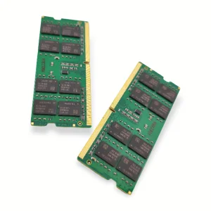
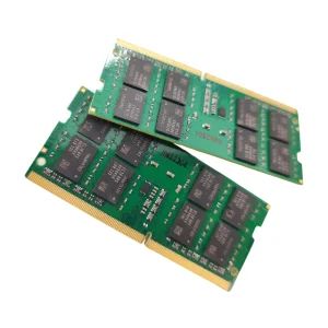
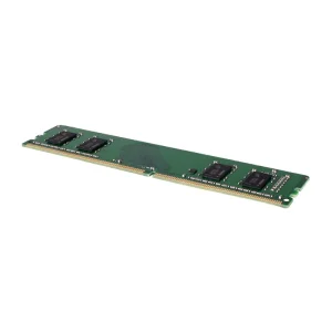
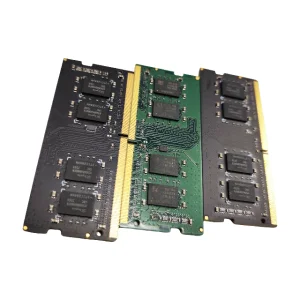
From prototype boards to production-grade server memory modules, we deliver consistent electrical stability.


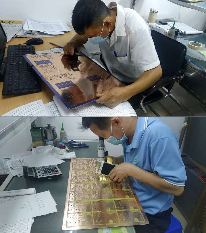
An engineering deep-dive on mechanical integrity, trace optimization, and thermal layout considerations.
Designing circuits for robust applications in hot, humid climates like Singapore requires careful consideration of board construction. Choosing between single-sided and double-sided boards involves balancing material limits, thermal coefficients, and high-frequency routing needs.
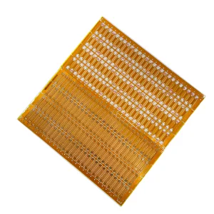
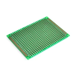
Single-sided printed circuit boards place all conductive copper traces on one side of the dielectric substrate, while components reside on the opposite side. While simple, they are the standard for low-density, cost-sensitive, and high-current power systems.
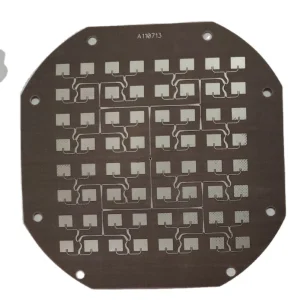
Double-sided PCBs utilize top and bottom copper layers connected via plated through-holes (PTH) or microvias. This layout allows for complex routing paths, localized ground planes, and higher design density.
Detailed technical answers to common fabrication, shipping, and engineering design queries for Singapore.
For standard double-sided and single-sided PCB prototypes, our express routing line delivers completed boards in 3 to 4 working days. Bulk production volumes typically ship within 7 to 10 days, utilizing direct airfreight to Singapore Changi Airport to minimize customs processing times.
We apply high-grade Electroless Nickel Immersion Gold (ENIG) or Immersion Silver surface finishes. These protect exposed copper traces from oxidation, ensuring robust solder joints and a shelf-life exceeding 12 months under tropical storage conditions.
Yes. Every Gerber package submitted undergoes a thorough DFM check by our 180-engineer R&D team. We verify drill-to-copper clearances, trace widths, thermal relief sizing, and soldermask alignments to eliminate manufacturing issues before fabrication begins.
Our partner manufacturing facilities operate under ISO 9001:2015 and ISO 14001 quality/environmental management systems. All materials are UL certified (UL 94V-0 flammability rating) and comply with international RoHS and REACH restrictions for toxic materials.
Yes. We stock various RF laminates, including Taconic TLY-5 (0.254mm) and Rogers 4003C/4350B. These are ideal for high-speed telecommunications and radar systems deployed by local Singapore aerospace and defense contractors.
We test 100% of our production runs using a combination of fly-probe electrical testing, automated optical inspection (AOI), high-magnification microscopy, and environmental burn-in stress tests. This rigorous testing minimizes assembly-level failure rates.
Established in 2016, NexaRAM Storage Technology Co., Ltd. has grown from a specialized DRAM storage developer into a global provider of memory modules and custom PCB assemblies. With 12 years of industry experience, the company serves as a strategic technology partner for global OEMs, system integrators, and industrial manufacturers.
Operating a modern 320㎡ facility and generating approximately USD 12 million in annual export revenue, NexaRAM combines precision manufacturing with rigorous testing protocols. The company uses automated optical inspection (AOI) and burn-in reliability testing to ensure high yield rates across all double-sided, single-sided, and multilayer PCB assemblies.
By leveraging a network of over 850 strategic partners, NexaRAM guarantees stable material sourcing and competitive pricing. This supply-chain depth allows us to deliver reliable electronic components to clients throughout North America, Europe, the Middle East, and Southeast Asia—with a dedicated focus on the Singapore market.
Get in touch with our engineering team today. Submit your Gerber files or design specifications, and receive a comprehensive DFM report and pricing quote within 12 hours.