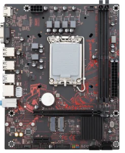
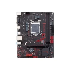
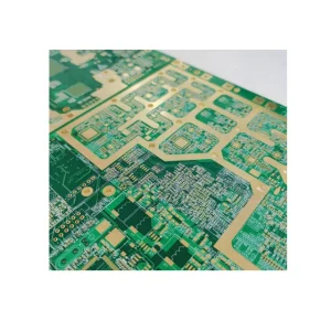
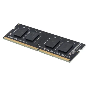
NexaRAM NexaRAM

Laser Stencils Exporter & Exporters for Russia

Precision Engineering, Advanced Solder Paste Deposition, and Robust Global PCBA Supply Chain Solutions

Laser Stencils in the Russian Industrial & Technology Sector

Current Landscape of SMT Manufacturing in the Russian Federation

Russia's electronics manufacturing landscape is undergoing a significant transition. Driven by structural requirements to localize hardware production and achieve technology independence, manufacturing hubs in St. Petersburg, Moscow, Novosibirsk, and Ekaterinburg are expanding their Surface Mount Technology (SMT) assembly capacities. Key industries driving this surge include industrial automation systems, transport electronics, agricultural monitoring technology, telecommunications, and advanced computing hardware.

In SMT assembly, the solder paste printing phase dictates over 65% of all PCBA defect rates. As Russian electronics manufacturers transition from legacy designs to dense, double-sided, multi-layered boards featuring fine-pitch BGAs (Ball Grid Arrays), QFNs, and ultra-miniature passive components (such as 0201 and 01005 packages), the quality of SMT laser stencils becomes a critical factor. Consequently, Russian assemblers rely on highly precise laser stencil exporters to supply custom-engineered stencils that meet tight dimensional tolerances and surface roughness requirements.

Technical Breakdown of Modern SMT Laser Stencil Engineering

Modern high-precision laser stencils exported to Russia are typically fabricated from specialized, stress-free tensioned stainless steel foils (specifically grade SUS304 or fine-grain steel). Laser cutting is performed using state-of-the-art fiber laser cutting machines, which minimize the heat-affected zone (HAZ) and deliver extremely clean, tapered aperture walls. The taper, typically between 1 to 2 degrees, is critical for clean solder paste release.

Key technical specifications demanded by Russian engineers include:

  • Aperture Aspect and Area Ratios: Standard ratios must adhere strictly to IPC-7525B guidelines, where the Area Ratio (aperture opening area divided by the surface area of the aperture walls) must exceed 0.66, and the Aspect Ratio must exceed 1.5 to guarantee stable paste transfer.
  • Step-Up / Step-Down Configurations: By etching or milling selected regions of the steel sheet, exporters supply multi-thickness stencils that deliver different solder paste volumes to different parts of the same PCB (e.g., standard deposition for passives, thick deposition for connectors, and micro-deposition for fine-pitch BGAs).
  • Advanced Nano-Coating: A hydrophobic and fluxphobic nano-coating applied to the contact side of the stencil reduces cleaning cycles from once every 3-5 prints to once every 15-20 prints, while preventing bridging, cold solder joints, and voiding.

Why Precision Metrics Matter

Solder paste release is highly dependent on aperture wall roughness. Fiber-laser cutting ensures a roughness parameter (Ra) of less than 1.5 µm, which is further reduced through electrochemical polishing processes.

Stepped Stencil Advantage

For Russian telecommunication PCBA designs containing both high-power components and high-density chips, step stencils optimize solder paste volume distribution on a single squeegee stroke.

Local Compliance (EAC & GOST)

Exporters must align their shipment documentation with Eurasian Economic Union requirements, assuring trouble-free customs entry and complete technical conformity for commercial factories.

NexaRAM Storage Technology Co., Ltd.

Industrial Showcase: High-Performance Memory SMT & PCB Assembly Integration

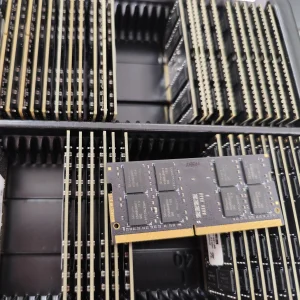
NexaRAM Storage Technology Co., Ltd. is a professional DDR5 memory manufacturer specializing in high-performance RAM solutions for global OEMs, data centers, and enterprise computing applications. Established in 2016, the company has rapidly developed into a reliable supplier in the advanced DRAM industry.

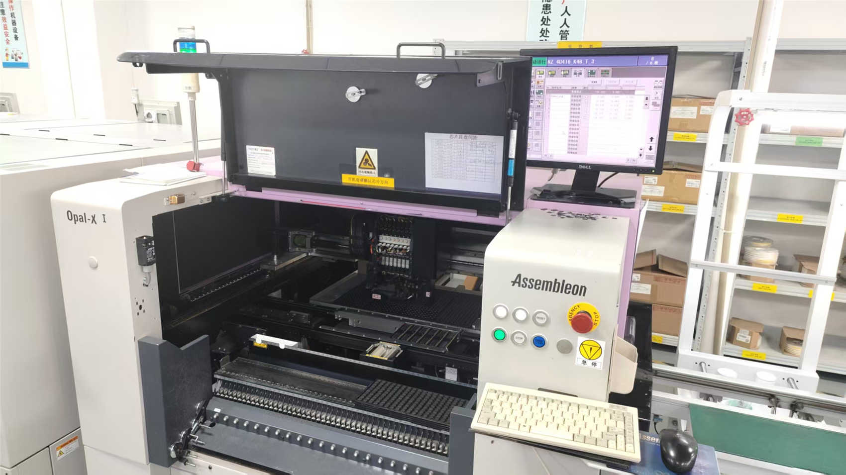
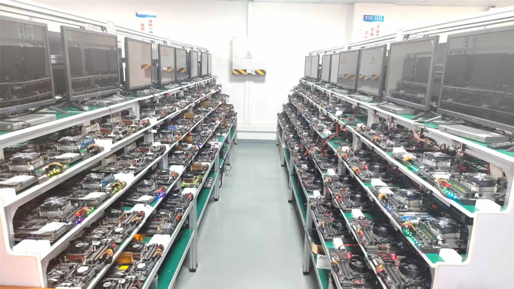
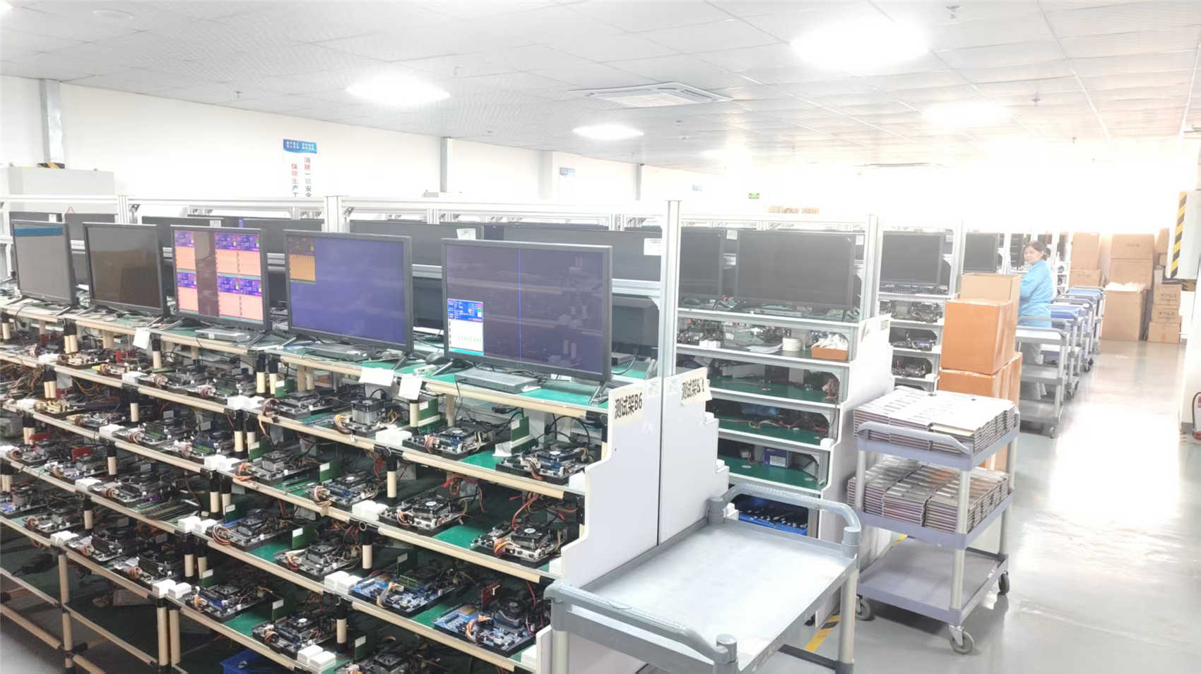
The company operates a modern production facility with a total building area of approximately 320㎡, equipped with advanced manufacturing and testing equipment to ensure stable and efficient production capacity. NexaRAM has an annual export revenue of approximately USD 12 million, with 6 years of export experience and 12 years of industry experience in memory and semiconductor-related fields.

Quality is strictly controlled through a combination of automated optical inspection (AOI) and burn-in reliability testing, supported by a professional QC team of 35 inspectors. The company follows international trade compliance standards and operates under a strong global trading background, serving markets across North America, Europe, Southeast Asia, and the Middle East.

NexaRAM maintains a highly developed supply chain ecosystem with over 850 strategic supply chain partners, enabling stable sourcing of high-grade semiconductor materials and components. Its primary customer base includes OEM manufacturers, system integrators, server solution providers, and gaming PC brands.

The company demonstrates strong R&D capabilities, offering custom DDR5 module design, PCB layout optimization, frequency tuning, and thermal solution development. Flexible customization options include frequency, latency, capacity, heat spreader design, and branding services. In the past year, NexaRAM launched 120 new product variants, supported by a dedicated R&D team of 180 engineers, continuously driving innovation in high-speed memory solutions for next-generation computing systems.

12M+

Annual Export Revenue (USD)

850+

Strategic Supply Partners

180+

Dedicated R&D Engineers

100%

EAC & GOST Documentation Ready
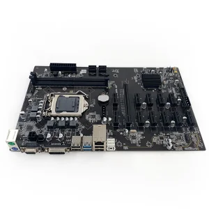
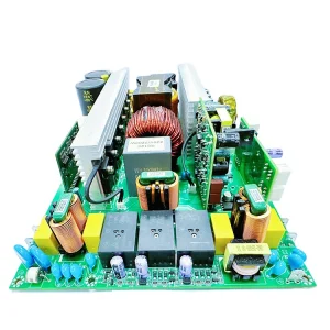
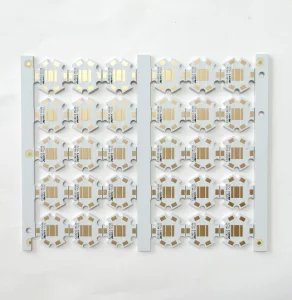
Technological Innovation & China-Russia Supply Chain Synergies

China's Manufacturing Capacity and Exporter Resilience

China remains the global nucleus for high-precision PCB and stencil fabrication. Equipped with industrial laser platforms (such as LPKF and Tannlin systems) that deliver automated aperture checking, Chinese fabrication facilities supply stencils with tolerances within ±2 µm. Additionally, our mature logistics channels, including direct rail transport through the China-Europe Railway Express (Новый шёлковый путь) and dedicated air cargo gateways in Moscow and St. Petersburg, offer swift and secure delivery. Standard stencils can be fabricated and dispatched within 24 to 48 hours of design approval, significantly minimizing downtime for Russian EMS factories.

Technical Roadmap: The Future of Solder Paste Deposition

The electronic hardware market is demanding denser layouts. Looking ahead, the stencil technology roadmap focuses on:

  • Electroformed Stencils (E-Form): Built atom-by-atom via nickel electrodeposition, electroformed stencils feature extremely smooth aperture walls, making them ideal for ultra-fine-pitch applications (under 0.3mm pitch) and advanced flip-chip assemblies.
  • Hydrophobic Polymer Nano-Coatings: Next-generation coatings bonded at the molecular level resist wear from harsh solvent wipe cycles, ensuring long-term paste release quality over high-volume production runs.
  • Integrated 3D Stencil Printing: Using multi-level step designs, 3D stencils accommodate complex PCB topologies, including pre-mounted components or high-density cavities on the board.

Trade Compliance & Logistics for Russian Operations

Exporting industrial machinery and precision tools to Russia requires strict adherence to customs regulations. Laser stencils must be classified correctly under HS Code 8442.50.10 (Printing plates, cylinders, and other printing components) or alternative metal classifications. The accompanying documentation must include full specifications of the stainless steel alloy, certificate of conformity (EAC), complete packing lists, and detailed technical drawings. Our logistics framework ensures all shipments are packed in heavy-duty wooden crates or protective cases with moisture absorption cards, preventing any warping or surface damage during transit.
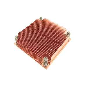
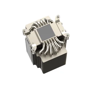
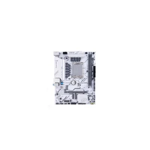
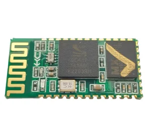
Frequently Asked Questions (FAQ)

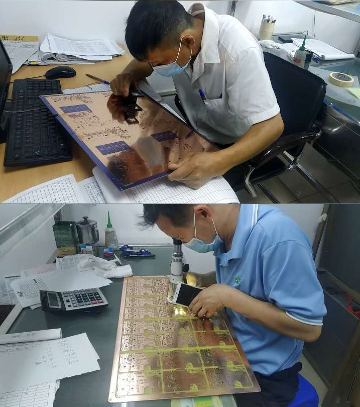
Expert technical insights regarding SMT laser stencils, exporting parameters, and localized production in Russia.

Q1: What is the optimal aperture modification strategy for printing solder paste on ultra-fine-pitch BGAs?
For Ball Grid Arrays with pitch under 0.5mm, we generally recommend reducing the aperture size by 10% to 15% compared to the copper pad dimensions. The shape of the aperture should ideally be rounded or square with radiused corners to promote clean corner release. Furthermore, maintaining an Area Ratio greater than 0.66 is necessary to prevent solder bridging or insufficient solder paste volume.
Q2: How does electropolishing improve SMT stencil performance?
Electropolishing is an electrochemical process that smooths the microscopic burrs and ridges left on the aperture walls by the laser cutting process. By reducing the surface roughness (Ra value) of the vertical walls, the friction coefficient between the solder paste and the aperture walls is lowered. This results in significantly improved paste transfer efficiency and cleaner deposit profiles.
Q3: What are the transit routes and lead times for shipping laser stencils to Russian SMT assembly facilities?
Standard air express delivery from our facilities to major Russian transport hubs (such as Moscow Sheremetyevo or St. Petersburg Pulkovo) typically takes 5 to 7 working days. For bulk industrial shipments, rail freight via the China-Europe Railway Express offers a cost-effective alternative with a transit time of 15 to 20 days, depending on the destination terminal.
Q4: What compliance documentation is required for custom clearance in the Russian Federation?
Customs clearance requires an accurate HS code classification (typically 8442.50.10 for printing components or 7326.90.98 for miscellaneous steel articles), a commercial invoice, a packing list showing net and gross weights, and a certificate of origin. Compliance certifications (such as EAC declaration of conformity) may also be required depending on whether the frame features pneumatic tensioning systems.
Q5: When should an SMT engineer specify a step-up or step-down stencil?
A stepped stencil is ideal when a PCB layout has mixed component densities. For example, if a board features large connectors requiring high solder volumes next to fine-pitch QFN or BGA components that require very small volumes, a stepped stencil can meet both needs. The step-down section reduces the thickness of the foil in the BGA area, preventing bridging, while the rest of the board receives standard solder paste volume.
Q6: What is the typical life expectancy of a nano-coated laser stencil?
Under optimal maintenance conditions—using soft squeegees, neutral cleaning solvents, and automatic under-stencil cleaning—a high-quality nano-coated stencil can deliver up to 50,000 to 80,000 printing cycles. The physical stencil foil can last longer, but the nano-coating layer may degrade after repeated contact cycles with aggressive chemical solvents.
Q7: How do you verify the dimensional accuracy of exported laser stencils?
Every stencil undergoes Automated Optical Inspection (AOI) before shipment. An high-resolution inspection system scans the entire stencil surface, comparing the laser-cut apertures against the original Gerber layout file. Any deviation in aperture width, position, or wall cleanliness is detected, ensuring 100% compliance with design specifications.
Q8: Which stainless steel alloys are recommended for SMT stencils?
We primarily use SUS304 and high-hardness fine-grain stainless steel. Fine-grain alloys are particularly suitable for high-density, multi-layer PCBs and micro-BGAs because their microstructure permits cleaner cuts and reduces mechanical deformation under squeegee pressure.
Q9: Can you manufacture framed and frameless stencils?
Yes. We supply framed stencils mounted on aluminum frames, which are ready to load into automatic printers. We also export frameless foils for use with quick-mount tension systems (such as ZelFlex or VectorGuard), which significantly reduce shipping volumes and costs.
Q10: What are the main causes of solder paste bridging, and how can the stencil design help prevent them?
Solder paste bridging is typically caused by excessive paste deposition, poor paste release, or incorrect stencil alignment. This can be resolved by using laser-cut stencils with electropolished apertures to ensure clean release, reducing aperture sizes relative to the pads, and choosing an appropriate foil thickness to control the volume of paste deposited.