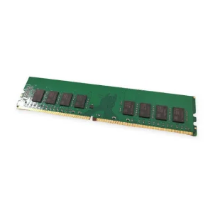
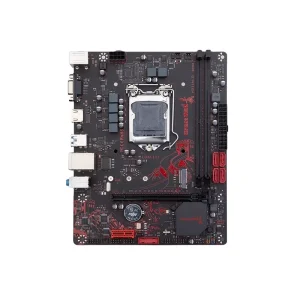
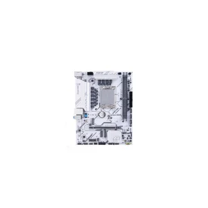
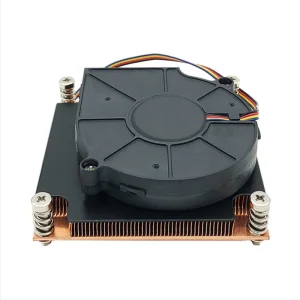
Explore our foundational system components engineered for extreme deployment reliability and signal integrity in computational infrastructures.
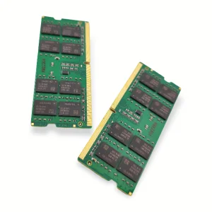
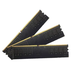
NexaRAM Storage Technology Co., Ltd. stands at the forefront of advanced memory architectures, operating as a specialized high-performance DDR5 and DDR4 DRAM module manufacturer. Engineered to support the intense architectural changes within the enterprise compute, mobile workstation, and edge server domains, the enterprise fulfills complex system requirements for Tier-1 global OEMs, hyperscale data centers, and multi-region electronics system integrators.
Established in 2016, NexaRAM has constructed an extensive technical framework rooted in semiconductor engineering excellence. Over a trajectory that bridges 12 years of industry experience in high-frequency signal design and memory sub-system manufacturing, the corporation has engineered robust supply paths and verification procedures. The operational infrastructure maintains an optimized, technologically integrated fabrication footprint spanning a modern production area of approximately 320㎡. This tightly curated, high-density manufacturing cell utilizes advanced clean-room protocols, high-precision automated surface-mount assembly, and complex diagnostic arrays.
Driven by an international operational model, NexaRAM achieves an annual export revenue of approximately USD 12 million. Backed by 6 years of continuous export execution, the company manages cross-border regulatory policies seamlessly, supplying robust product suites across critical global trade zones including North America, Europe, Southeast Asia, and the Middle East.
Analyzing the transition from legacy high-speed DDR4 signaling to next-generation intelligent DDR5 and CAMM2 topologies within modern corporate mobile compute platforms.
Unlike standard DDR4 memory where error correction requires an independent DRAM component handled by an enterprise-level memory controller, DDR5 implements intrinsic On-Die Error Correction Code (ECC). This architecture isolates single-bit errors inside the silicon die itself, mitigating systemic failure risks during dense computing workloads, optimizing yield, and scaling stability down to sub-14nm lithographies.
Modern mobile platforms require extreme power efficiency. The transition from DDR4 to DDR5 shifts the critical power management architecture off the system motherboard and directly onto the memory PCB substrate via an integrated Power Management IC (PMIC). This enables refined 1.1V rail granularity, minimizes thermal dissipation across laptop motherboards, and enhances overall signal cross-talk margins.
DDR5 modules introduce an updated bus architecture, modifying the standard single 64-bit data channel found on DDR4 SO-DIMMs into two fully independent 32-bit subchannels (plus an extra 8 bits for ECC in enterprise modules). This duplication optimizes command bus efficiency, reduces data access latency, and unlocks structural throughput limits for multi-threaded AI processing pipelines.
Aligning manufacturing capabilities with procurement logic to address supply vulnerability, engineering customizations, and cost targets for global procurement officers.
Within the highly volatile global semiconductor supply chain, multi-national hardware procurement managers face continuous pressures: balancing component cost targets against strict operational reliability parameters. Sourcing memory modules for industrial mobile devices, field-deployed laptops, medical diagnostic systems, and edge data terminals requires complete transparency into raw silicon origin, tiering frameworks, and manufacturing traceability.
NexaRAM addresses these enterprise pain points directly through a deeply integrated B2B supply infrastructure. Recognizing that component failure in enterprise laptop deployments can lead to significant warranty costs and localized downtime, our procurement logic guarantees:
Detailing the precision testing configurations and production workflows behind NexaRAM's memory solutions.
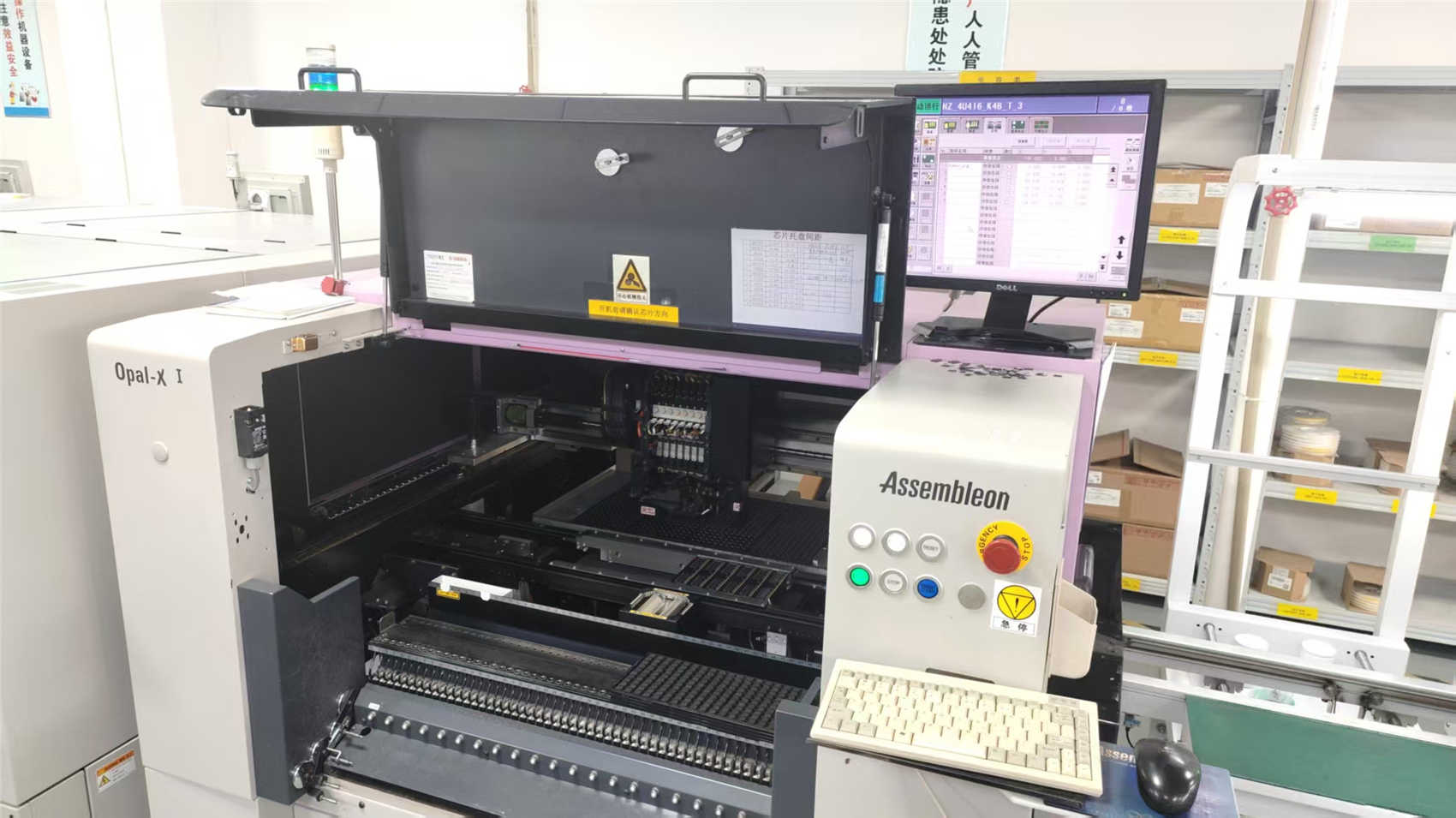
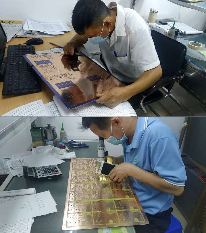
The foundation of NexaRAM's operational authority is a robust engineering capability driven by a dedicated R&D group comprising 180 experienced semiconductor engineers. This core engineering unit handles custom high-frequency PCB layouts, thermal stress simulations, and multi-platform motherboard compatibility validation. Over the past single-year product release cycle, this R&D infrastructure designed and brought to market 120 distinct product variants, expanding our coverage across specialized capacities, form factors, and latency matrices.
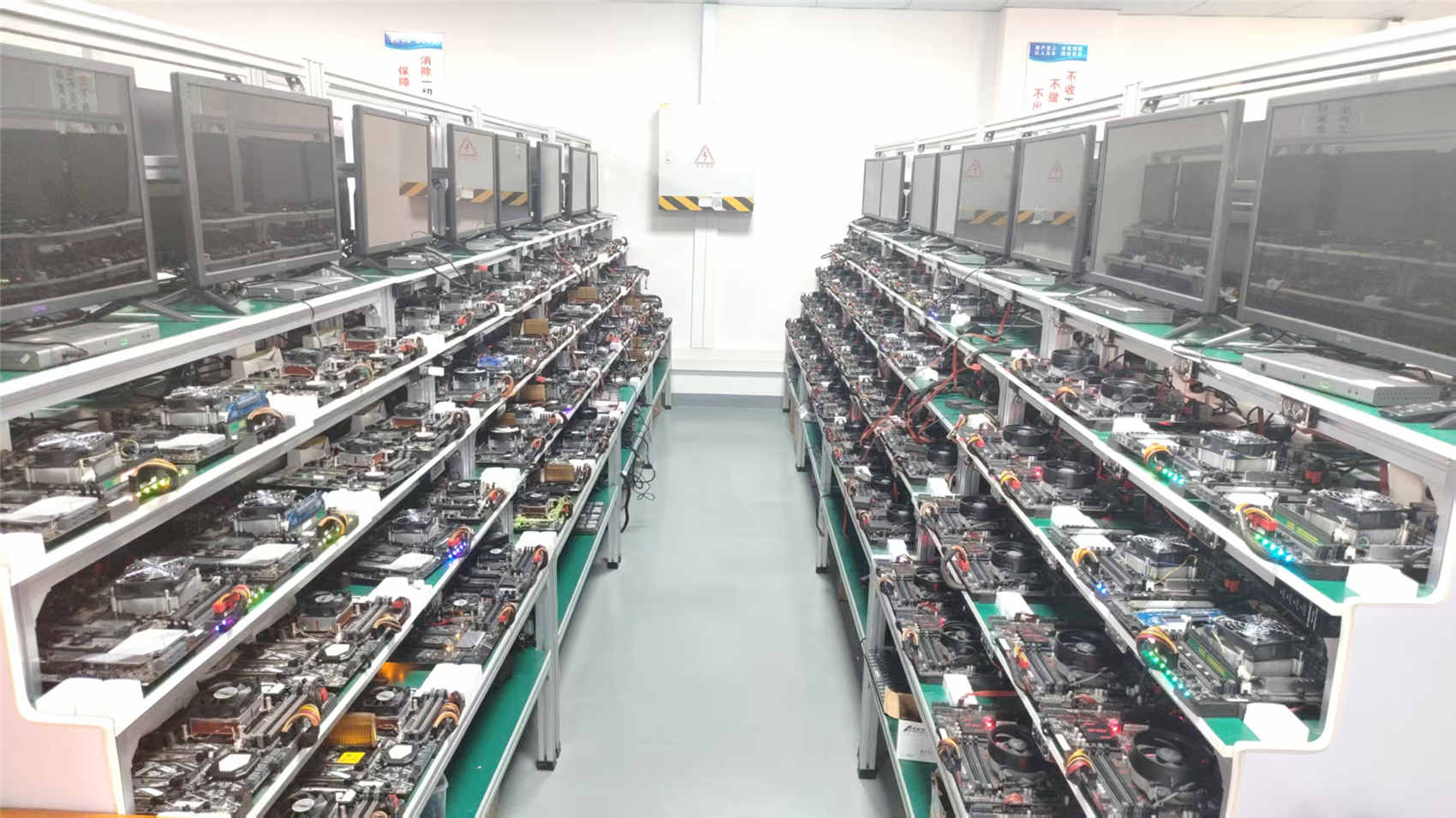
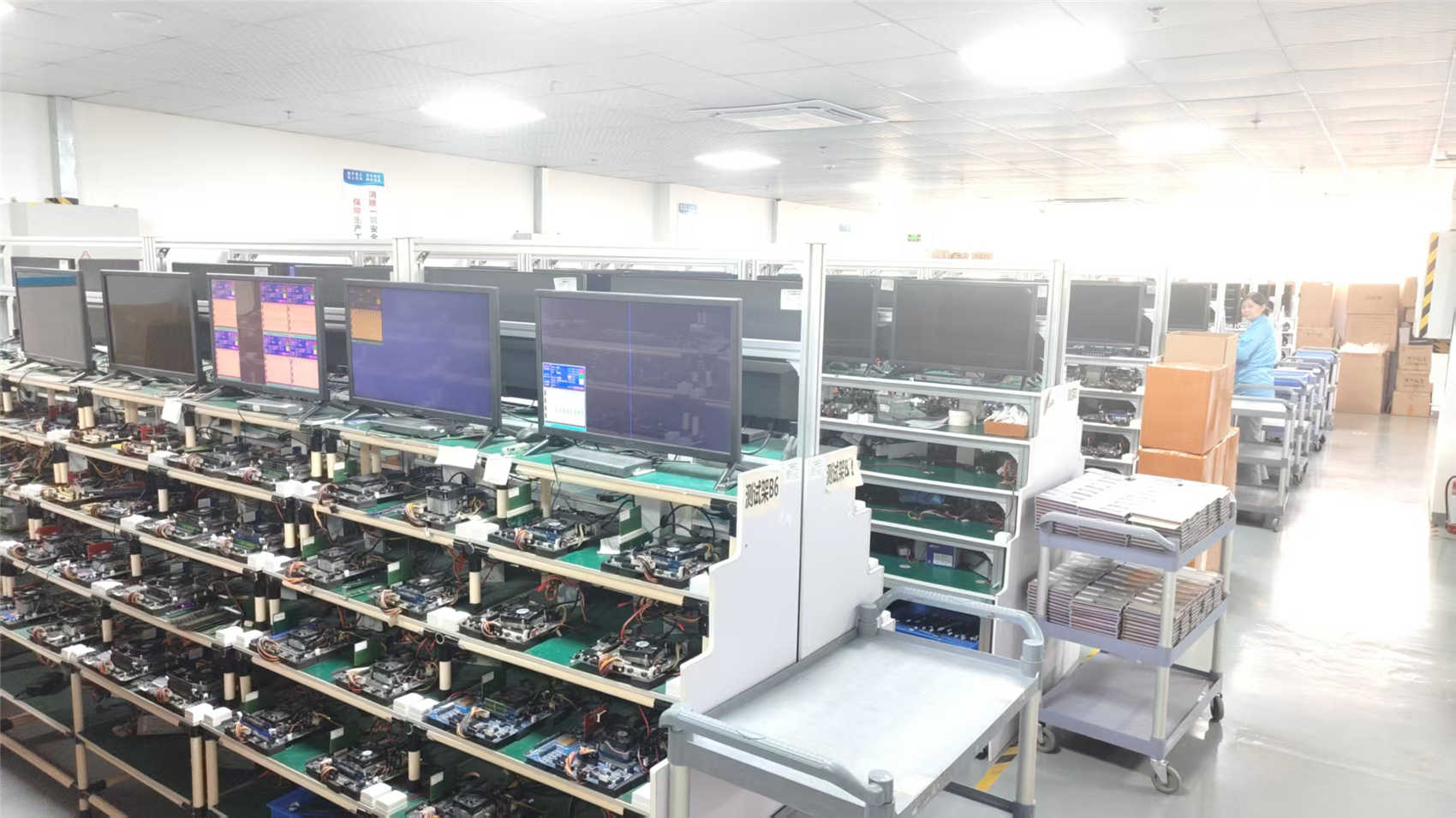
To guarantee flawless execution at scale, quality management is governed by a technical team of 35 specialized QC inspectors and quality metrologists. Every memory module undergoes a strict multi-stage testing process before packaging and international shipment:
High-throughput multi-angle automated cameras rapidly inspect 100% of finished assemblies. This process identifies component misalignments, micro-voiding within the BGA solder balls, passive component structural anomalies, and solder bridge imperfections down to micron-level tolerances.
To eliminate early component mortality, modules are subjected to continuous thermal stresses in specialized environmental chambers. Operating under high voltage conditions at 85°C for extended testing blocks, this process forces latent defects to manifest prior to final product verification.
Every batch undergoes strict hardware verification utilizing advanced electronic diagnostic equipment. This environment evaluates signal eye-diagram parameters, data setup and hold time windows, and physical signal transmission lines over diverse system environments.


Ensuring complete regulatory compliance across major international markets through formal quality and environmental auditing certifications.
International microelectronics distribution requires absolute adherence to environmental, safety, and supply chain regulatory structures. NexaRAM builds confidence into every transaction by maintaining full compliance matrix alignment with key regulatory standards including CE, FCC, RoHS, and REACH. This ensures our clients face no regulatory roadblocks when deploying products across European, American, or Asia-Pacific markets.
Operating a diverse supply framework with over 850 strategic supply chain partners, we enforce ethical sourcing and conflict-free mineral guarantees throughout our upstream materials network. Our comprehensive trade framework handles complicated cross-border documentation, customs clearance parameters, and bonded warehouse fulfillment seamlessly, offering reliable, predictable logistical timelines to hardware production facilities worldwide.
An authoritative engineering outlook tracking the upcoming convergence of high-speed memory modules, CAMM2 packaging architectures, and the rise of local AI computing platforms.
The continuous evolution of client hardware demands a profound shift in modern memory subsystem architectures. The rapid integration of local neural processing units (NPUs) within next-generation corporate laptops—designed to run large language models locally—demands unprecedented data bandwidth directly from the system RAM pool.
To support this high-performance computing shift, NexaRAM's engineering teams are re-allocating design resources toward ultra-low power consumption and shorter signal pathing. By managing signal routing layout distances down to sub-millimeter tolerances, we continue to successfully unlock higher performance margins. This relentless technical innovation ensures our OEM/ODM customers maintain a distinct edge, equipping them to power the future of high-speed AI and enterprise mobile computing.
Direct technical answers addressing the critical product validation, quality assurance, and manufacturing parameters required by commercial procurement managers.
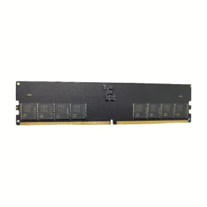
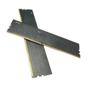
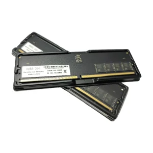
High-reliability structural components, high-frequency enterprise memory modules, and multi-layered processing hardware optimized for industrial ecosystems.